In this theory, we will examine a component widely used in electronics : the transistor.
The main manufacturing processes of the transistors will be exposed as well as the fundamental assemblies.
1. - THE JUNCTION TRANSISTOR :
It is a device formed of three semiconductor zones arranged next to each other so that two consecutive zones are of different type.
With this system, it is easily understood that only two types of the above device can be obtained : either a semiconductor zone P is inserted between two semiconductor regions N as shown in Figure 1-a, or On the contrary, an area N is inserted between two zones P (Figure 1-b).
The devices in question are then supplemented by three metal plates placed respectively on the ends of the lateral zones and on the side of the central zone. They are designated by the letters E, B, C.
To distinguish the two types, the device of Figure 1-a is called NPN transistor and that of Figure 1-b PNP transistor.
On the other hand, in both cases, the central zone is called the base (hence the symbol B given to the plate and the corresponding link) while the lateral zones are called emitter and collector respectively (hence the symbols E and C given to platelets and corresponding links).
The characteristics of the two types of transistors are similar, that is, they function in the same way. However, they require voltages of opposite polarity : the NPN transistor operates with positive voltages while the PNP transistor operates with negative voltages.
(We report the same diagram above to make reading easier, ie figure 1).
Looking at Figure 1, we see that the three zones form two distinct junctions ; in the NPN transistor, the emitter and the base form an NP junction while the base and the collector form a PN junction.
In the case of the PNP transistor, however, the emitter and the base form a PN junction while the base and the collector constitute an NP junction.
When no voltage is applied to the electrodes of the transistor, that is to say when its two junctions are not polarized, the same phenomena appear in the PN junction. (See semiconductors 3).
Each junction is the seat of a potential barrier where zone N is made more positive than zone P. The potential barrier has a value such that it allows the passage of a majority carrier stream equal to the flow of carriers minority. Thus the total flow of the carriers through each junction is zero.
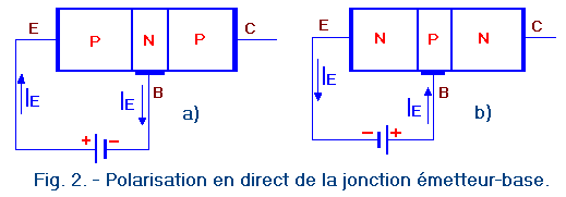
For normal operation of a transistor, whether PNP or NPN, the emitter-base junction must be forward biased while the collector-base junction must be reverse biased. The polarization of the junctions can be obtained by means of a properly connected battery.
To directly polarize the emitter-base junction, the cell is connected as shown in Figure 2-a in the case of a PNP transistor, or as shown in Figure 2-b in the case of an NPN transistor.
In the circuits thus formed, in a similar manner to what happens in a diode, a direct current called emitter current is circulated and designated IE.
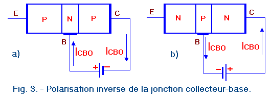
In order to reverse bias the collector-base junction, the cell is connected as shown in Figure 3-a in the case of a PNP transistor, or as shown in Figure 3-b in the case of an NPN transistor.
In these new circuits, one also observes what happens in a diode, that is to say that one sees the circulation of a reverse current called residual current and designated by ICBO.
This symbol (ICB0) indicates that this is the current flowing through the collector-base junction when the emitter-base junction is not polarized (IE = 0).
The residual current ICB0, due to the minority carriers, has a very low intensity. This, which does not depend substantially on the voltage applied to the collector-base junction, is largely dependent on the temperature at which the transistor is located and its characteristics.
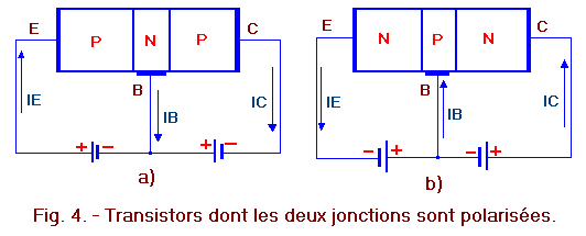
From what we have just said, it follows that each junction of a transistor behaves like a diode. This is only true if the two junctions are polarized separately. If against, they are polarized simultaneously as shown in Figure 4, the behavior of the transistor is different.
In this case, indeed, currents IE and ICB0 do not continue to flow independently of one another as shown in Figures 2 and 3.
When the two junctions are polarized as illustrated in Figure 4, the resulting current ICB0 increases to reach a value almost equal to that of the current IE : this new current is called the collector current and is designated by IC. It can thus be seen that in a transistor, the emitter current can influence the collector current.
Thus, when the emitter current is zero as in the case of Figure 3, the collector current has a very low intensity (it is the residual current ICB0). When, on the other hand, the emitter current is no longer zero, as in the case of Figure 4, the collector current increases by a value almost equal to that of the emitter current. To explain it, we must consider the inside of the transistor.
Let us first examine the PNP transistor of Figure 4-a by looking at the emitter-base junction.
Since this junction is forward biased, the two flows of the majority carriers that pass through it are much more intense than the two minority carrier streams. These will be neglected. There will therefore be a stream of holes flowing from the transmitter to the base and a stream of electrons flowing from the base to the transmitter. The electrons reached on the transmitter recombine in turn with the holes present while so many electrons are provided at the base by the battery connected between this base and the transmitter.
Simultaneously, the same stack attracts an equal number of electrons from the transmitter in which new holes are formed replacing those that have disappeared due to recombinations with the electrons from the base. On the other hand, the flow of holes flowing from the transmitter to the base behaves in a completely different manner. Indeed, it is necessary to know that the holes reached in the base become minority carriers since this base is of type N.
On the other hand, the collector-base junction being polarized in reverse, this polarization stops the flow of the majority carriers while it favors the passage through the junction of the flow of the minority carriers. As a result, the holes from the transmitter that have reached the base are forced to cross the collector-base junction as well. These holes, minority carriers, thus join the collector.
It therefore adds, to the small residual current of the minority carriers crossing the collector-base junction polarized in reverse, much more intense current due to the holes coming from the transmitter.
Previously, we said that the collector current increases by a value almost equal to that of the emitter current. Indeed, all the holes coming from the transmitter do not reach the collector because a small part of them recombines with the electrons present in the base. This thus contributes to forming the basic current designated IB as shown in Figure 4-a
(We report the same diagram above to make reading easier, see figure 4).
To make the collector current as equal as possible to the emitter current, it is necessary to try to minimize the number of holes recombining with the electrons present in the base.
For this purpose, the transistors are made with a very thin base so as to reduce the path that the holes perform to reach the collector.
The possibility that these holes have to meet the electrons present in the base and recombine with them becomes weaker.
For this reason, in the figures considered so far, the area constituting the base is represented narrower than the other two forming the emitter and the collector. Another way to reduce this possibility of encounter is to realize this base with a semiconductor slightly doped. Thus, the number of free electrons present in the base is reduced.
The transmitter is so called because it emits the holes that, after crossing the base, arrive at the collector. Its name comes from the fact that it "collects" most of the holes "emitted" by the transmitter.
What has been said is valid for the PNP transistor. The same can be said for the NPN transistor of Figure 4-b, taking into account that in this case the emitter consists of an type N semiconductor. Thus, it "emits" electrons which are, for much, "collected" by the collector after crossing the base.
Since the electrons have a charge of opposite sign to that of the holes, the two cells with which the NPN transistor is biased are connected with the opposite polarities of those adopted for the PNP transistor. As a result, the emitter, base and collector currents are oriented in opposite directions as shown in Figure 4-b.
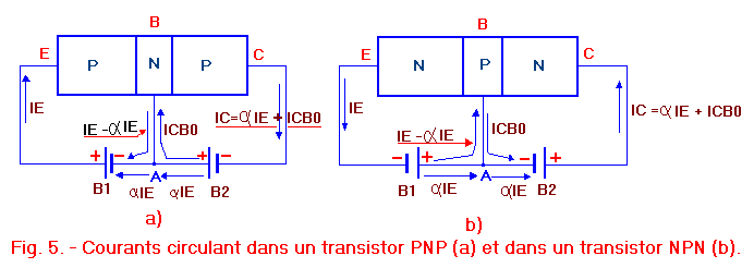
Now, we will specify the composition of the collector and base currents by referring to a PNP transistor.
As we have said, the collector current IC is formed of the residual current ICB0 and largely of the emitter current IE.
The current IC, being a little lower than the current IE, is expressed by means of the product of the current IE by a factor slightly lower than 1 called coefficient of amplification current and which is designated by the Greek letter (alpha). The value of the coefficient The value of the coefficient depends on the manufacturing characteristics of the transistor ; it is generally between 0.920 and 0.998. Thus, the portion of the emitter current that reaches the collector of a transistor can be calculated by the product
x IE.
Example : if the coefficient has a value of 0,98 and the emitter current IE is 5 mA, he above product becomes x IE = 0,98 x 5 mA = 4,9 mA
; this means that a current of 4.9 mA reaches the collector.
By adding the residual current ICB0 to this current, the collector current IC is obtained ; the expression of the latter is therefore IC =
x IE + ICB0.
As can be seen in Figure 5-a, the current IC at the output of the collector passes through the stack B2 and reaches the point A where it splits in two. One part, constituting the current ICB0, returns to the base while the other part (x IE) goes to the battery B1 of the emitter current IE.
At point A, the current IE is added to the current indicated in FIG. 5-a by IE - x IE. current that does not reach the collector because of the recombination of holes and electrons in the base. This current, denoted IE
-
x IE, is precisely equal to the difference between the emitter current IE and a part of this current (that is to say
x IE) which reaches the collector.
In Figure 5-a, it can thus be seen that the base current, that is to say the current flowing in the connection connecting the point A to the base of the transistor, is formed of two currents : the current ICB0 who enters the base and the current that comes out :IE - IE . Since generally the latter has a value greater than the ICB0 current, the base current IB is directed in the direction indicated in Figure 4-a, that is to say outgoing from the base, so in the same sense as the current IE - IE.
What has been seen above for the PNP transistor is also valid for the NPN transistor provided that the direction of all the currents is inverted. As seen in Figure 5-b, this is due to the reverse polarity of the two batteries.
From what has been said so far, it is not yet possible to deduce what the practical utility of the transistor may be ; for the moment, we have found that the current IC can be controlled by means of the emitter current IE. However, we have seen that the latter is larger than the first and therefore, from this point of view, we find no advantage.
But we must not reason only by running ; the tensions involved must also be taken into account. Indeed, it must be remembered that the emitter-base junction is forward biased whereas the collector-base junction is reverse biased.
It follows that, in order to cross the emitter-base junction by the emitter current IE, it suffices to apply a reduced voltage : consequently, the power involved in the emitter circuit is rather low. On the other hand, since the collector-base junction must be reverse biased, it can be applied to a voltage greater than that applied to the other junction.
The collector current IC being very little less than that of the emitter IE, the power involved in the collector circuit is therefore greater than that to the emitter circuit.
It can thus be said that a transistor behaves like an amplifier because by providing its input circuit with a low power, it is able to provide in its output circuit a power that can be a hundred times greater. This is due to the fact that the transistor has the property of circulating in the high voltage output circuit the same (or almost) current as that flowing in the low voltage input circuit. Indeed, if the collector-base voltage was less than or equal to the emitter-base voltage, the power of the output circuit would be less than that supplied to the input circuit and therefore power amplification could not be possible.
The necessary condition for an amplified transistor is therefore that the collector circuit operates at a voltage much higher than that at which the transmitter circuit operates. Thus, if a low-power signal is applied to the input of a transistor, the same signal can be taken from its output circuit, but this signal has a much greater power.
One can take as mechanical analogy the compressed air brake of a coach ; the driver would not be able to exert sufficient force to block the wheels, so he is limited to controlling with his foot a pneumatic valve regulating the inflow of compressed air. This one is able by against, to exert on the brakes the force necessary to the stop of the vehicle.
The transistor behaves like a valve. Indeed, using a small power (supplied to the transmitter circuit), one can control a power in the much larger collector circuit.
It can also be noted that the emitter circuit has a low resistance (it behaves in fact as a diode in direct polarization) while the collector circuit has a much greater resistance.
From this point of view, the transistor is a device capable of transferring a certain current from the low resistance input circuit to the high resistance output circuit. This property was indicated by the Americans in condensed form by the words transfer and resistor which gave rise to the term transistor.
In the figures examined so far, the transmitter and the collector have always been represented as equal areas arranged on either side of the base area. In addition, the left zone has always been considered as emitter and the right zone as collector. Since these two zones are equal and arranged symmetrically with respect to the base, one could think that one can use as transmitter the zone of right and as collector that of left. In other words, one might think that the transmitter and the collector of a transistor are interchangeable, that is to say that the transmitter can perform the function of the collector and vice versa.
In fact, the emitter and the collector are made differently although they are semiconductors of the same type.
Thus, for the amplification coefficient to be as close as possible to 1, significantly different doping is performed for the semiconductor which will have to function as an emitter and for the one which will have to perform the collector function.
The transmitter will be the most heavily doped semiconductor ; in addition, to facilitate the dissipation of heat developing inside the transistor, the collector-base junction is made with a larger section than that of the emitter-base junction.
We will review some processes used for the fabrication of transistors.
The first transistors were built according to the same principle as that used for diodes with tip ; thereafter, from 1950, other methods were used which can be reduced to three: the alloy process, the diffusion process and the planar process.
The alloy junction technique essentially involves contacting a semiconductor chip with a certain amount of impurity material and heating the material to a temperature above its melting point. An alloy formed by the impurity material and the superficial portion of the semiconductor is thus formed.
After cooling of the alloy and the pellet, a certain amount of impurity atoms form in the semiconductor crystal lattice an N-type or P-type zone distinctly distinct from the remainder of the pellet. If the pellet is of N type, impurity materials are used which, after cooling, give a zone P. Conversely, if the pellet is of the P type, impurity materials are used which are capable of determining the formation of a zone N.
The junction between the area that has formed and the rest of the pellet constitutes a PN junction.
To obtain a transistor, it is necessary to form in the same pellet two PN junctions ; therefore, the same treatment is performed simultaneously on the two opposite sides of the same pellet so as to create the two required junctions.
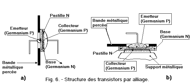
Figure 6 shows the sections of two alloy transistors ; these are germanium PNP transistors formerly used in amplitude modulated radio receivers and in low frequency amplifiers.
The transistor of Figure 6-a, has been manufactured to function as a voltage amplifier in the low frequency preamplifier stages, in the oscillator stages and in the medium wave converters, or in the intermediate frequency amplifiers ; the same structure has been adopted for the manufacture of certain types of transistors used in the final stages of power amplifiers less than 1 Watt.
The transistor of Figure 6-b was, on the other hand, made to function as a final low frequency amplifier for powers equal to or greater than 1 Watt.
Both structures were obtained with the same alloy process in N germanium single crystal pellets.
These pellets constitute the base electrode ; the zones P, arranged on both sides on the opposite sides of the pellet, form the emitter and collector electrodes.
Each pellet is welded to a pierced metal strip ; the emitter electrode is in the center of the hole so that the transmitter is not in contact with the band.
In the structure of Figure 6-b, the electrodes have larger dimensions than those of Figure 6-a ; this has been done so that they can be traversed by more intense currents without there being an excessive heating. Furthermore, still in the structure of Figure 6-b, the collector electrode appears mounted on a fairly large metal support ; this arrangement has been adopted to increase the power dissipated by the transistor during its operation.
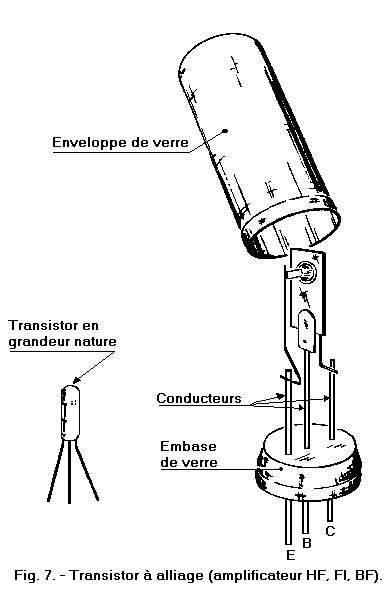
In Figure 7, one can see how are arranged the transistors (those of the type of Figure 6-a) in their glass envelope.
The outer surface of the envelope and the lower part of the base are generally covered with black paint which is intended to prevent the light can have an influence on the operation of the transistor.
The inside of the housing is filled with silicone grease, which is used to prevent surface damage to the semiconductor and to dampen any mechanical vibrations.
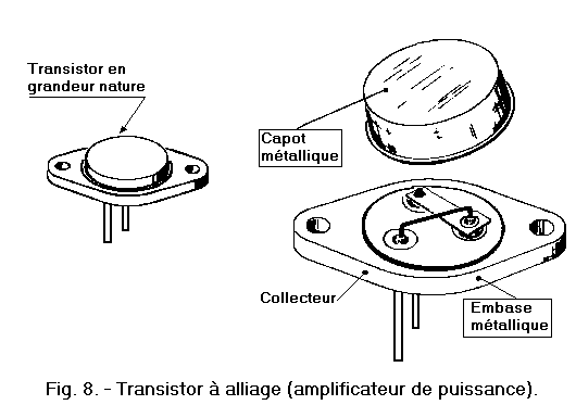
If it is a power transistor, it covers the envelope of a metal cylinder which not only protects the transistor from light, but also serves to improve the heat dissipation.
Figure 8 shows a power transistor of the type shown in Figure 6-b.
The entire base and cover form a metal housing that has a good heat dissipation capacity generated by the transistor. To improve the heat dissipation, directly welds the collector electrode, which is the most subject to heating, to the base.
In this way, it can serve as a radiator and replaces the terminal of the collector (C) which is apparently absent. The transistor thus conditioned has a robust, compact structure and therefore particularly resistant to different thermal and mechanical stresses.
With the technique of alloy junctions, it has been possible to manufacture PNP transistors operating up to 15 MHz and NPN transistors operating up to 30 MHz.
In general, the response of a transistor to the high frequencies depends on the transit time of the electric charges constituting the current in the base, that is to say the time that the electrons spend to cross the P-zone of the NPN transistor or the holes to cross the N zone of the PNP transistor. By reducing this transit time, the frequency response of the transistor is improved.
The reduction of the transit time in the base can be obtained in two ways : the thickness of the base and therefore the path of the charges is reduced, or the speed of these charges is increased.
The minimum base thickness obtained by the alloy junction method is of the order of one micron (10-6 meters) ; but even with these extremely small dimensions, it is not possible to achieve sufficiently short transit times to have alloy transistors operating at frequencies above 30 MHz.
To further improve the frequency response of the alloy transistor, technological tricks are used to accelerate the charges in the base electrode.
The acceleration of the charges is obtained by progressively graduating the concentration of the impurity atoms along the thickness of the pellet intended for the fabrication of the alloy transistor. Thus, in the base that retains the original structure of the pellet, there is a gradient in the concentration of impurity atoms from the emitter to the collector : this gradient is called the "impurity gradient".
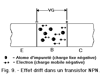
In Figure 9, one can see schematically the gradient of impurities in the base of a transistor ; indeed, the impurity atoms are more numerous on the transmitter side and their number decreases when approaching the collector.
Recall that the base of an NPN transistor, such as that shown in Figure 4-b above, is constituted by a P-type semiconductor, that is to say by a semiconductor in which the atoms of impurities have acquired an electron. These atoms are therefore negative fixed charges.
The higher density of impurity atoms on the transmitter side than on the collector side causes a greater concentration of negative charges on the transmitter side than the collector. Thus, some VG potential difference exists between the ends of the base.
This difference in potential, due to the degradation of impurities, is oriented so that it exerts a force on the mobile charges, that is to say the electrons passing through the base. This results in a greater acceleration of these charges and consequently a reduction in their transit time.
This phenomenon is commonly called "drift effect" (drift is an English term meaning thrust, drift).
Different types of high frequency alloy transistors have been manufactured on the basis of the drift effect. They have been used in the high and intermediate frequency stages of the AM - FM radio receivers and televisions and many others ...


 Transistors with alloy junctions
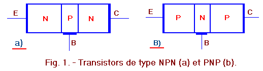
 Click here for the next lesson or in the summary provided for this purpose.
 Top of page
 Next Page