We will now observe the behavior of two type N and P semiconductor crystals when one of their ends is fused together.
We will examine their properties and the applications that result from them.
1. - THE JUNCTION P.N.
We already know that type P crystals contain holes as majority carriers while type N crystals contain free electrons as the majority carriers.
Let us see the behavior of the majority carriers when a junction is formed between two semiconductors of different types, that is to say between a crystal P and a crystal N (Figure 1-a).
In practice, the junction is established by forming, by special technical means, a zone P in a single crystal N or conversely a zone N in a single crystal P. On the other hand, it is impossible to unite two crystals of different types to form a single crystal. PN junction
However, in order to better understand what happens at a junction, we will represent the latter by the union of two different germanium plates.
When the junction is carried out, part of the free electrons of the crystal N, under the effect of thermal agitation, begins to spread in the crystal P and at the same time, still under the pressure of the thermal agitation, a part holes of the crystal P propagates in the crystal N.
At first, the diffusion of electrons and holes is done with a certain regularity in both directions. Theoretically, if we maintain this rhythm for a sufficiently long time, we arrive at a final state in which the free electrons and the holes are uniformly distributed in the two crystals. In reality, the diffusion stops, well before occupying the two crystals completely and thus, there is formed around the junction surface a single (relatively thin) zone, in which the free electrons and the electrons are mixed in equal quantities. holes.
In the final phase, we thus obtain three distinct zones :
- A zone N : constituted by the part N of the crystal, not occupied by the holes coming from the crystal P.
- A zone P : constituted by the part of the crystal P not occupied by free electrons from the crystal N.
We finally find on the edges of the junction surface, the new zone that we can call "intrinsic", considering that it contains an equal number of free electrons and holes (Figure 1-b). However, this new area should not be considered as intrinsically intrinsic. Indeed, the distribution of the free charges is not uniform as in the intrinsic semiconductors. To qualify this phenomenon, we use the English name depletion region, which can be translated by zone of exhaustion, recalling that in the area in question, the diffusion thrust of the free charges from the two crystals together, s'exhausted.
By examining the phenomena that arise immediately after the formation of a PN junction, we have so far limited ourselves to observe the displacements of free electrons and holes, without taking into account the crystalline reticles in which the diffusion takes place charges. In fact, the two crystalline reticles exert a great influence on the diffusion. Indeed, it is from the electrical characteristics of the reticles that is born the biggest obstacle for the completion of the diffusion of the charges in the two crystals.
When the electrons coming out of the crystal N enter the reticle of the crystal P and the holes emerging from the crystal P propagate in the reticle of the crystal N, two new electrical states occur at the ends of the two reticles in contact. Indeed, on the end of the crystal N, a positive electricity accumulation is formed, due to the loss of electrons and the acquisition of holes, whereas at the end of the crystal P, we find a Negative accumulation of electricity, due to the loss of holes and the acquisition of electrons.
The separation of the charges of opposite signs produces an electric field E, circulating from the positive end of the crystal N to the negative end of the crystal P (Figure 1-b) and we report the same diagram in order to simplify your task and especially of understand the process).
This electric field acts to oppose the diffusion of the charges through the junction, insofar as it tends to bring the holes of the crystal N to the crystal P and the electrons of the crystal P to the crystal N.
With the increasing intensity of the E-field and the spreading of charges continuing, the load-return force also increases. Thus, the thrust of diffusion will find more and more opposition, until the equilibrium between the opposing forces is reached, thus causing the cessation of any diffusion of the charges in the two crystals.
With the equilibrium established between the force of the electric field and the diffusion thrust, a separation of a certain quantity of positive and negative charges is also formed on the two edges of the zone of exhaustion. Therefore, at the edges of the latter, a certain potential difference (Vo of Figure 1-b) remains constant and for this reason it is commonly called but improperly, contact potential or diffusion potential.
In the future, when we talk about this potential difference Vo, we will use the denomination potential barrier. This term, more correct than the previous one, recalls the obstacle that the potential Vo represents, for the subsequent diffusion of the electric charges from one crystal to another.
It is therefore from this potential barrier Vo which is formed at the junction P.N. that all the properties of the crystal diode depend.
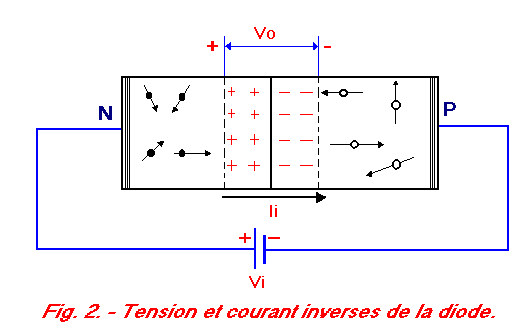
After examining the formation of a junction between two semiconductors of different types, let us now see the behavior of this one when it is polarized, that is to say when the voltage delivered by a continuous power supply is applied to both areas of the crystal.
The voltage can be applied in both directions, that is to say, by connecting the positive pole of the cell to the zone N and the negative pole to the zone P or vice versa, by connecting the positive to the zone P and the negative to the zone N.
In the first case, we say that the junction (that is to say the diode) is reverse biased while in the second case, the diode is forward biased.
What happens at the PN junction when it is reverse biased ?
Figure 2 shows that at the instant when the circuit is closed, a portion of the free electrons is detached from the zone N of the crystal and moves towards the positive pole of the battery supply.
At the same moment, a certain quantity of electrons emitted by the negative of the battery, joins the zone P of the crystal, where they will make disappear some of the holes.
If now we admit that in zone P there are no free electrons that can join zone N to replace those which are pushed towards the positive of the pile and that in zone N there is no holes that can spread to the P area to replace those that have disappeared, we could conclude the cessation of the movement of the charges from the crystal to the battery and the battery to the crystal. Indeed, the number of free electrons present in the N zone of the crystal is undeniably very large, but not unlimited ; it is the same for the holes present in the crystal P.
The cancellation of the current produced by the battery, immediately after the closing of the circuit, is justified by the fact that the electrons and the holes are in limited number in one or the other of the crystal and by the impossibility to replace them when they move away and disappear.
In reality, the displacement of the charges and consequently the current produced by the battery, ceases even before the zone N is released from its electrons and the zone P of its holes.
To explain this phenomenon, let us know that the potential barrier is rapidly increasing with the decrease of free electrons and holes in the respective zones and its amplitude increases by passing from Vo to Vo' (compare on this subject Figures 1-b and 2).
The new potential difference Vo' can thus cancel the effect of the external voltage Vi, before all the electrons of the zone N are pushed towards the positive of the battery and before all the holes of the zone P have faded away.
The voltage Vi applied across the diode (Figure 2) is called reverse voltage. If one takes into account what has been said previously, the current flowing in the diode (at the terminals of which a reverse voltage has been applied) should be canceled rapidly. In reality, the current does not cancel out completely due to the presence of the minority carriers, that is to say the presence of holes in the zone N of the crystal and free electrons in the zone P.
A certain number of minority carriers still manage to cross the junction, thus causing a partial replacement of the free electrons in the zone N and holes in the zone P. We thus see the presence of a very weak current, flowing from the end N at the P end of the crystal. This current is called reverse current (Ii).
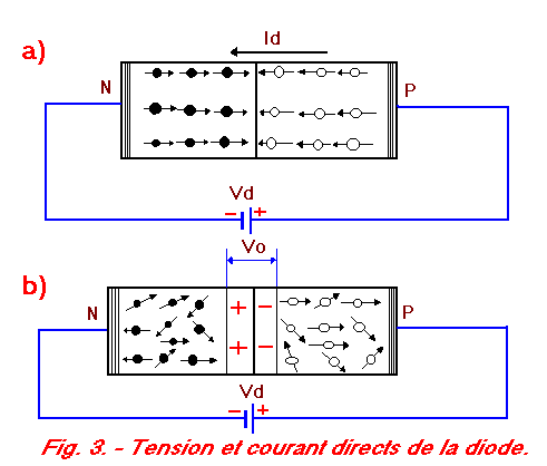
Let us now see the opposite phenomenon, that is to say when the P.N. junction is forward biased (Figure 3-a).
When the circuit is closed, the electromotive force of the battery sets in motion the free electrons of the zone N and the holes of the zone P, which converge both towards the junction (Figure 3-a), inside which the electrons fall into the holes, which causes the disappearance of each other. However, the free electrons that fall into the holes are continually being replaced by others, coming from the negative of the power source.
Thus, all the missing holes are replaced by others, which are formed on the side of the zone P, towards the positive of the battery. The flow of charges is therefore reproduced perpetually, forming a continuous current. It can also be seen by measuring the direct resistance of the diode.
The direct current Id is said direct current, the external voltage, Vd which is at the origin of the formation of the current Id, is said direct voltage.
Figure 3-b illustrates the case where the DC voltage Vd is lower than the potential difference Vo (Figure 1-b), which constitutes the potential barrier. Thus, as long as the voltage Vd is less than or equal to Vo, the current is practically zero. This current practically only exists when the voltage Vd exceeds the value of Vo. This value differs according to whether the junction is constituted by a germanium crystal or by a silicon crystal : for germanium, this value is normally 0.2 to 0.3 V whereas for silicon it is 0.6 at 0.7 V.
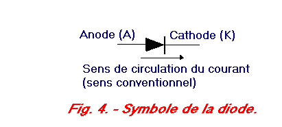
A junction P.N. allows the passage of a current when it traverses the semiconductor in the direction of the doped crystal P to the doped N. It opposes the flow of a current in the opposite direction.
The P.N. junction in germanium or silicon can be used to produce a device called a diode whose graphic symbol is shown in Figure 4. The conduction of the diode is indicated by the direction of the arrow.
The anode (A) corresponds to the zone P of the junction and the cathode (K) to the zone N ; the "A" end requires a positive voltage with respect to the other end "K".
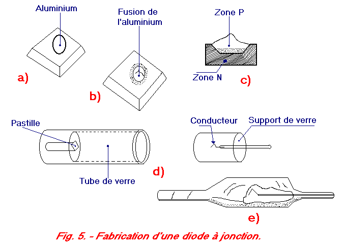
The junction is obtained by laying on a semiconductor chip N, a certain amount of aluminum (Figure 5-a) or indium ; the whole is heated to obtain the melting of aluminum or indium, and the partial melting of the semiconductor (Figure 5-b). After cooling, these bodies solidify forming a zone P for aluminum and the junction P.N. in the pellet N (Figure 5-c).
The whole is then introduced into a glass tube (Figure 5-d) and the conductor is welded to aluminum or indium (Figure 5-d on the right). The glass tube is closed to form the housing of the diode (Figure 5-e). There are also other methods of manufacturing the diodes. For example, to obtain the P.N. junction, reference can be made to the diffusion method which consists in evaporating impurities so that they enter the pellet P so as to form an zone N.
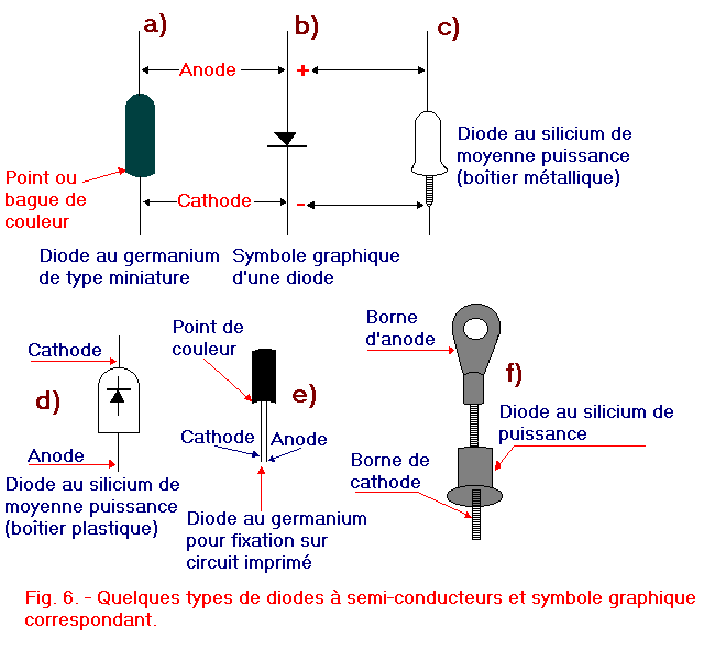
Diffusion is used in the manufacture of silicon diodes that can withstand high voltages and currents. Figure 6 illustrates some types of semiconductor diodes. The cathode of the diodes of Figures 6-a and 6-e is indicated by a ring or dot of color on the component housing.
In Figures 6-c and 6-d, we have two other types of silicon diode acting as a rectifier. These rectifying diodes are in these figures in a metal case or in a plastic case.
Despite their reduced size, some diodes provide high currents (more than 10 amperes) and can even function properly at a very high ambient temperature (150°C).
The diode of Figure 6-c, which is widely used in radio and TV receiver power supplies, can be attached to the chassis of an apparatus by means of nuts and washers as well as that of Figure 6-f used for very high powers where a heat sink is needed.
The electrical characteristics of the component, given by the manufacturer, are valid only for a determined ambient temperature because if the latter varies, the values of the diode change substantially.
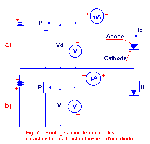
To obtain the voltage current characteristic curve of a diode, two electronic assemblies are used :
- The first one (figure 7-a) makes it possible to obtain the direct characteristic of the diode. For this, using a potentiometer that is varied, we apply a direct voltage Vd, measured by the voltmeter (V) and we note the corresponding values of the direct current Id on the milliammeter (mA).
- The second (Figure 7-b) provides the opposite characteristic of the diode. For this, the assembly remains the same with the only difference that the battery and the two measuring devices are connected in reverse. It should be noted that the use of a micro-ammeter (µA) facilitates low reverse current (Ii) measurements.
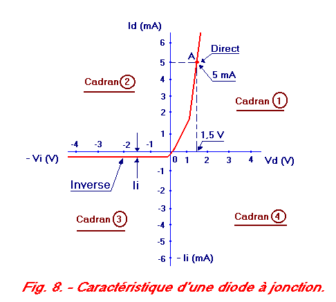
Each pair of measured values (voltage and current) can be plotted on a graph with two orthogonal axes graduated (Figure 8), the first horizontal in volts, the second vertical in milliamperes.
Taking as an example the pair of values : Vd = 1.5 V and Id = 5 mA, we obtain on the graph a point A corresponding to the intersection of the two dashed straight lines starting perpendicularly from the very place where they are carried values.
By reporting point by point each pair of values obtained in the corresponding dials on the graph (direct voltages and currents in the dial "1", voltages and reverse currents in the dial "3" and connecting by a line all these points, obtains the characteristic curve of a type of diode (Figure 8).
We can notice that the curve passes through the origin of the axes (point 0) ; a zero voltage causes the absence of current.
In the dial "1", it is observed that the current and the voltage increase or decrease together.
For each type of diode, the manufacturer sets a maximum value (Idmax) not to exceed without risk of damaging it. It also indicates the repetitive peak current that the diode can withstand for short periods of time at determined time intervals and the non-repetitive peak current that the diode receives once in a while, for example when powering up.
These last two values are higher than that of the current (Idmax) which represents 20 to 30 times less the value of a non-repetitive peak current.
In the dial "3", it is noted that the reverse current (Ii) is practically constant and that it does not depend on the inverse voltage (Vi) when the latter varies over a certain range. The reverse voltage of a diode can reach a few hundred volts up to a limit value (Vimax) imposed by the manufacturer beyond which the diode is destroyed.
As long as this value is not reached, the reverse current of the diode remains low and therefore it can not occur a breakdown of the junction of the diode.
In summary, the constructor provides the following characteristics :
- Maximum forward current (Idmax) Generally noted by IF (English literature : "forward").
- Repetitive peak current (IFRM).
- Peak overload current (non-repetitive) IFSM
- Maximum reverse voltage (Vimax) Generally noted by VR (English literature : "reverse"
- Peak reverse peak voltage VRM
- Continuous reverse current IR (the lower the current, the better the diode quality).
A power diode that provides a high Idmax current can not have as low a reverse current as the one that only supports a few tens of milliamperes and yet the quality is not affected. It is good to know what temperature is the junction of the diode when determining the value of the reverse current IR because it is derived from the concentration of minority carriers that are sensitive to thermal variations.


 Polarization of the junction
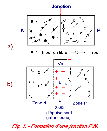
 Click here for the next lesson or in the summary provided for this purpose.
 Top of page
 Next Page