The explanation of current flow in a P-type semiconductor may seem complex, since it assumes conduction due to positive charges. However, the phenomenon is justified by the Hall effect measurements which show the displacement of positive charges (holes) in a P-type semiconductor.
The HALL effect (of the name of the scientist who discovered it) can be highlighted by the experiment shown schematically in figure 6.
Suppose first that a continuous voltage is applied to a conductive block made of ordinary material using two plates AA' and BB'. In this case, the current flowing through this block is formed of electrons flowing from BB' to AA'.
Then place the block in a uniform magnetic field, created by a magnet, so that the flux lines are perpendicular to the block.
The electrons circulating in the block are influenced by the magnetic field and tend to move in a direction perpendicular to that of their own motion and magnetic field lines.
In the case illustrated in Figure 6, where the electrons move from BB' to AA' while the lines of force go from the top (north pole) to the bottom (south pole), the charges tend to move to the right of their movement initial. As a result, these charges (electrons) are no longer uniformly distributed in the block, but focus on the side A'B'.
This accumulation of electrons produces an effect that can be demonstrated by a very sensitive voltmeter. Indeed, by connecting the device as shown in Figure 6, an electrical potential difference is measured: the side A'B' is negative relative to the side AB. This potential difference obviously comes from the concentration of electrons on the A'B' side.
The HALL effect consists precisely in this deformation of the current lines (electron flux), in a conductive plate under the effect of a magnetic field perpendicular to this plate. This effect is still true in the case of a semiconductor block N, because it is the electrons that form the most important current flow.
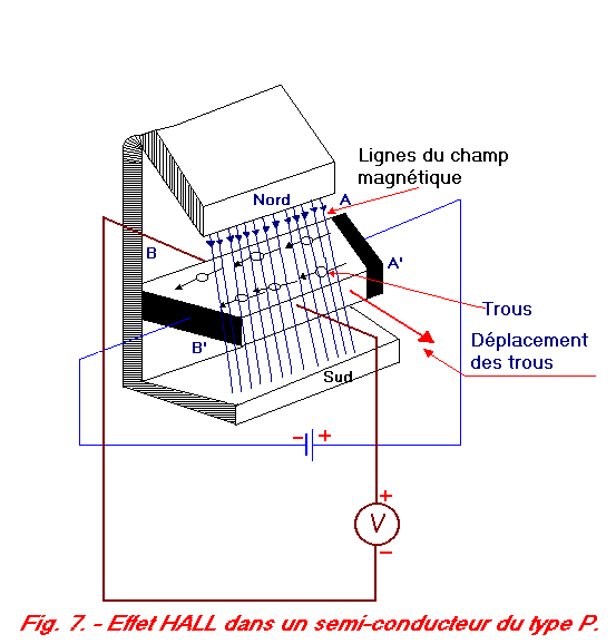
On the other hand, with a P-type semiconductor block (Figure 7), the voltage indicated by the voltmeter is of opposite polarity to that which one had with the ordinary conductive block or the On the other hand, with a P-type semiconductor block (Figure 7), the voltage indicated by the voltmeter is of opposite polarity to that which one had with the ordinary conductive block or the N semiconductor.
This result can only be explained if it is assumed that the moving charges are positive in the case of the P-type semiconductor.
They will be shifted, under the action of the magnetic field, to the left of the direction of their scrolling which is opposite to that of the electrons of Figure 6. This concentration of holes on the face A'B' also causes a polarity opposite of that which was present in the case of an ordinary conductor or a semiconductor. Thus, it is confirmed experimentally that the holes (positive charges) form the circulating current in the P-type semiconductors.
With the help of the HALL effect, it was also possible to measure the mobility of the charges in the two types of semiconductor.
The mobility expresses, in centimeters per second (cm / s), the speed of the charges moving in a semicircular cube of 1 cm of edge when the voltage applied on two opposite faces is 1 volt.
This measurement made it possible to determine that the electrons have a mobility greater than that of the holes (also called cavity or gap).
The average life of holes and free electrons is an important parameter that should not be neglected ; it corresponds to the interval of time which elapses between the moment when in the semiconductor the concentration of the holes and free electrons undergoes a variation, and that where it returns to the equilibrium conduction (recombination of the charges).
3. - PREPARATION OF SEMICONDUCTORS FOR ELECTRONIC USE
Germanium and silicon are the semiconductors most widely used in the manufacture of electronic components.
Germanium is found in the form of mineral salt in certain types of rock : coal (or fossil coal), zinc and cadmium ores.
Much of the germanium for electronic uses is extracted from the by-products of industrial transformations of blende (zinc ore) and fossil carbon (coal).
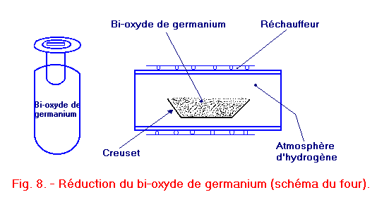
By subjecting the carbon soot and slag of the zinc ore to appropriate treatments, a germanium compound called germanium bi-oxide is obtained. The bi-oxide thus extracted is far from having the purity required. It contains many traces of foreign elements that must be removed by chemical means before extracting germanium. The purified germanium bi-oxide is placed in a crucible which passes into a furnace with a hydrogen atmosphere and at the outlet, germanium is obtained (Figure 8).
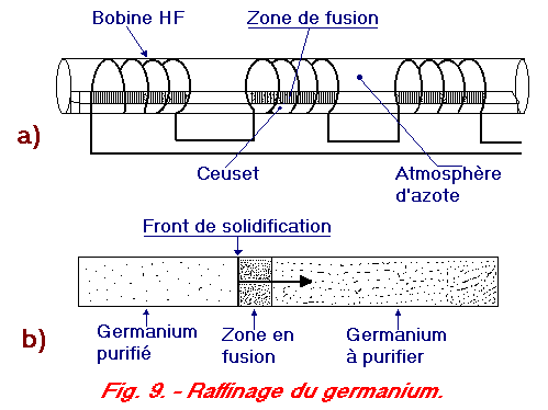
It has a white-silvery, shiny appearance ; it is already relatively pure, but not enough for use in the electronics industry. To obtain the desired purity, the germanium is placed in a graphite crucible, which passes slowly into a special tubular furnace, schematically illustrated in Figure 9-a.
The furnace consists of a long quartz tube, on which are coils traversed by a very intense current of high frequency. This current produces inside the furnace a particularly powerful variable magnetic field under each coil. Thus, in the germanium which is under the coils, there is a strong heating and a fast melting. The fusion of germanium remains limited to the areas placed under the coils. Therefore, as the crucible slowly advances from one end to the other of the furnace, the molten zones move in the germanium in the opposite direction to that of the crucible.
The solidification front which moves from left to right (Figure 9-b) following the melting zone can be compared to a porous filter which allows the germanium to pass, and keeps the impurities dissolved in the melted zone.
The operation is repeated under each coil, and at the outlet of the furnace, a germanium of a high degree of purity is obtained.
Like germanium, silicon intended for electronic uses must be very pure. Normally, silicon is extracted from silicon bi-oxide by carrying a sand-carbon mixture at a temperature of 3000°C.
The silicon obtained by this process contains 2 to 3% impurities, while for use in electronics this value must be less than 0.05%.
A certain degree of purity can be achieved by chemically treating the silicon with different acids.
For some time, however, we have obtained better results from the chemical treatment of a silicon salt instead of sand.
For the physical refining of silicon crystals, a variant of the method illustrated in Figure 9-a is used.
The silicon bar is placed in the vertical position in the center of a HF tube furnace.
Along the outer wall of the furnace, a coil is traversed by an intense HF current. In correspondence with this turn, a molten zone is formed in the silicon which moves in the bar from one end to the other. The filtering action is thus carried out in the same way as that described for germanium (Figure 9-b).
The process is repeated several times in order to obtain the necessary degree of purity.
After refining, the semiconductor is in the form of a solid aggregate, consisting of innumerable crystals, very small and arranged in all directions.
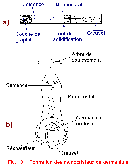
The semiconductor thus formed, although being very pure, is not yet usable for the realization of diodes and transistors. For these components, it is necessary to transform the aggregate into monocrystal, that is to say into a single and large crystal. Figure 10 illustrates two methods of forming single crystals of germanium.
The first method (Figure 10-a) is a new application of the oven HF (High Frequency) and the mobile zone melt.
The germanium bar obtained at the end of the refining is placed in a quartz crucible with a germanium monocrystal called seed and a layer of graphite. The crucible slowly advances into the furnace so that the molten zone moves smoothly from one end of the barrette to the other.
The melted part solidifies in the form of a single crystal oriented according to the crystalline reticle of the seed.
During the formation of the single crystal, metered quantities of foreign substances are introduced in order to transform the intrinsic semiconductor into P or N type semiconductors.
The most common substances used to form P-type semiconductors are indium, aluminum and gallium. For N type semiconductors, arsenic, phosphorus and antimony are used.
For the formation of the single crystal, it is also possible to proceed according to the method illustrated in Figure 10-b. The installation essentially comprises a heater, a crucible and a lifting shaft.
In the crucible is melted germanium and impurity materials necessary to achieve the types P or N Initially, the seed is placed in the lower part of the lifting shaft, and thus adheres thereafter to surface of the molten germanium contained in the crucible.
By adjusting the temperature, it is possible for the germanium to begin to crystallize at the point of contact with the seed. At this time, the uprising tree rises very slowly so that the forming crystal continues to grow.
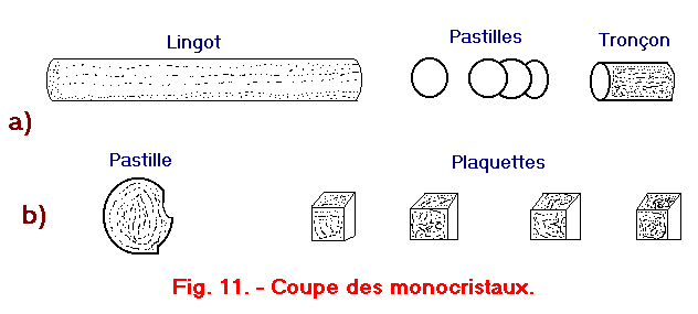
Generally at the end of this step, the single crystal is in the form of a cylindrical ingot. This one, after some checks concerning the perfect distribution of the impurities, is cut into very thin slats called pellets (figure 11-a). These pellets are flattened on both sides, polished with solvents and then cut into platelets (Figure 11-b).
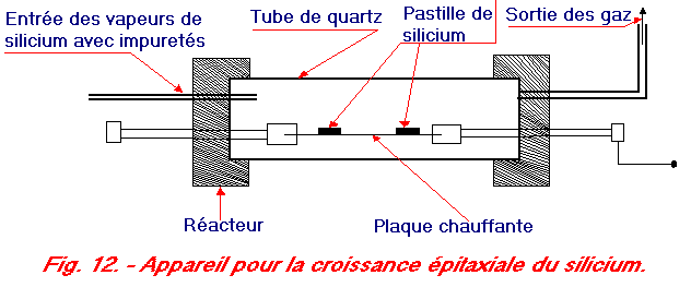
Another method of increasing a widely diffused crystal is that of epitaxial growth (Figure 12).
This technique makes it possible to deposit on the surface of a crystalline product another product which is brought to it in the form of vapor. The layer deposited on the surface of the so-called epitaxial layer product has the same doping as the vaporized product.
The crystalline epitaxial growth makes it possible to obtain the formation of very thin mono-crystalline layers with a thickness of about one micron (thousandths of a millimeter).


 Preparation of semi-conductors for electronic use
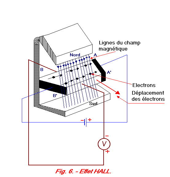
 Click here for the next lesson or in the summary provided for this purpose.
 Top of page
 Next Page