The Zener effect and the Capacity of the Junction :
4. - ZENER EFFECT
Figure 9 shows the typical typical curve of a junction diode. By examining it carefully, we note that the curve always passes through the axes, that is to say that in the absence of voltage applied across the diode, the current no longer passes.
The left side of the characteristic, corresponding to the reverse bias of the diode, shows that by increasing the negative voltage applied, the current becomes very low, even if we arrive at voltages of several volts. Indeed, the characteristic is always at the same distance from the horizontal axis (Figure 9).
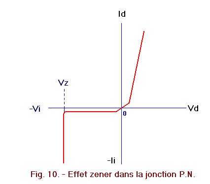
Given this, we can think that the reverse voltage can increase without limitation since the current, having reached the saturation limit (corresponding to the concentration of minority carriers) no longer increases. In reality, the current is constant only to a well-defined point in the voltage, after which it starts to increase very rapidly, so much so that the inverse characteristic changes from the almost horizontal position to the vertical position (Figure 10).
There is therefore a considerable increase in minority carriers and as a result, the reverse current becomes much more intense.
This phenomenon is called the ZENER effect, after the name of the scientist who discovered it and succeeds in explaining it.
The voltage at which the phenomenon occurs is called ZENER voltage (Vz of Figure 10).
To explain the ZENER effect, it is necessary to remember that when a diode is reverse biased, we have a reverse current, consisting of minority carriers, due to the formation of electron-hole pairs, caused by the breaking of existing links between the atoms of the semiconductor.
The rupture of the bonds is caused by the vibration of the atoms under the effect of the temperature. There are also other causes likely to cause the formation of an electron-hole couple.
By studying the P.N. junction, we have seen that near this junction, an area of free charges is formed (zone of exhaustion), to which corresponds a potential difference, called a potential barrier.
Since this area is excessively thin, increasing the reverse bias voltage of the diode causes an increase in the potential difference near the junction. This increase reaches such a proportion (Vz = tension of ZENER), that it generates a force able to remove from their orbit a large number of peripheral electrons, belonging to the atoms being close to the junction.
However, for each electron that moves away from its orbit, it appears an electron-hole pair, thus a considerable increase of the minority carriers.
The reverse current then becomes relatively intense.
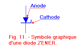
Diodes designed to take advantage of this phenomenon are called ZENER diodes (Figure 11). In these, there is also another phenomenon called the avalanche effect.
The avalanche effect occurs when the minority carriers present near the junction accelerate to such an extent that they strike the peripheral electrons of the atoms at a speed sufficient to detach them from their orbit.
The free charges thus obtained are accelerated and in turn produce (again by shock) new charges and so on. Thus, the number of free charges increase very rapidly, hence the name of avalanche effect given to this phenomenon.
Charges made free in this way increase the current due to the ZENER effect. This means that according to the voltage of ZENER (Vz), the reverse current passes very rapidly from a reduced value to a remarkably high value.
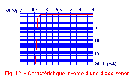
Figure 12 illustrates this phenomenon very well. It represents the appearance of the inverse characteristic of a ZENER diode.
As can be seen, the reverse current is at first so small (a few micro-amperes) that the characteristic is almost on the horizontal axis, from which it then detaches itself quite abruptly to practically go to the vertical state. Looking at the almost vertical part of the characteristic, tending to demonstrate that the voltage remains constant although the current varies within wide limits, it is understood that the ZENER diodes can be used as voltage stabilizers.
Indeed, after appropriate doping of the semiconductors, it is possible to vary within wide limits, the voltage for which the zener effect is verified. With such methods, it is possible to manufacture ZENER diodes, capable of stabilizing voltages of different order, ranging from a few volts to several tens of volts.
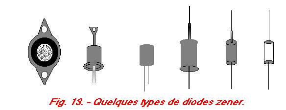
Figure 13 shows some commonly used types of ZENER diodes.
A P.N. junction has a resistance depending on the type of polarization applied to it :
- In direct polarity, this resistance has a low value.
- In reverse polarity, it is very large (apart from the ZENER diodes where the avalanche effect was caused).
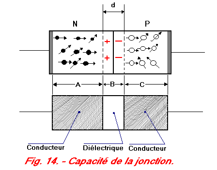
A careful examination of a junction shows the similarity with a capacitor. Indeed, if we consider an unpolarized P.N junction, three parts stand out (figure 14) :
- A (A) constituted by the semiconductor N
- Another (C) by the semiconductor P
- Finally a third (B) which is the potential barrier.
A material containing mobile charges can be likened to one conductor while another, deprived of these same charges, behaves like an insulator. Thus, the junction appears consists of two metal parts (A and C) separated by another insulator (B), similar to a dielectric.
It is known that two metal plates separated by an insulator (dielectric) constitute a capacitor and the junction of a diode is an example.
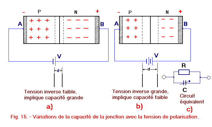
If at present a reverse bias is applied to the junction, the plates A and B are respectively rendered negative and positive ; the potential barrier increases and the capacity is modified (Figure 15-a).
Thus, depending on the value of the reverse voltage applied to the diode, the intrinsic capacitance thereof varies within certain limits (Figure. 15-b). The equivalent diagram of the diode in reverse is given in Figure 15-c.
A variable capacitance in parallel on a resistor of very great value to simulate the current leakage (some microamperes) of the dielectric.
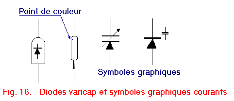
The property of the reverse junction allowed the realization of automatic frequency control circuits of oscillators (for example, local oscillators of FM or TV receivers).
Figure 16 represents two types of variable capacitance diodes (VARICAP), some of which have a capacity ranging from a few picofarads to about one hundred picofarads depending on the reverse voltage applied across the terminals.
Silicon rectification diodes, the most used, can also be used in variable capacity ; the parallel resistance (very large) does not disturb the oscillating circuits.
In direct polarization, the capacitance of the diode is "masked" by the resistance which is low in this case. The capacity of the diode can play a detrimental role in very high frequency arrangements where it is used for its recovery properties. Indeed, its reactance can become very weak and thus offer a short circuit to the reverse voltage. Its use is therefore to be avoided in these montages.
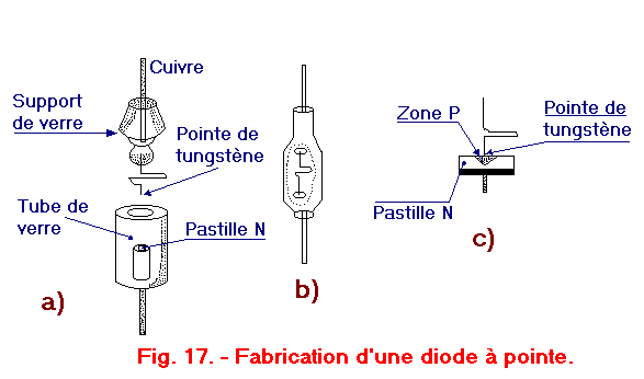
Designed before the junction diode, it is used for unidirectional conduction in direct polarization. It consists of a point contact, at the level of the semiconductor chip, by a very fine tungsten wire. At the time, electromagnetic waves (radio waves for example) were used to detect a galena crystal detector consisting of a piece of lead sulphide ore (galena) on which was placed what was called the "cat's mustache". Figure 17 illustrates the fabrication of a tip diode whose arrangement of the various elements hardly changes from that already seen for the junction diode.
After closing with the glass support (Figures 17-a and 17-b), a very high value current is passed through the tungsten tip and the n-doped germanium or silicon pellet for a short time. in order to create, by melting at the point of contact of these two elements, a definitive junction (Figure 17-c).
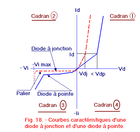
The shape of the characteristic of the diode tip is therefore substantially the same as that of the diode junction as shown in Figure 18.
However, there are some differences : in direct polarization (dial 1, Figure 18), for the same current in the two components, the voltage applied across the tip diode is greater than that of the junction diode. In sum, the tip diode has a higher direct resistance than the junction diode.
In inverse polarization (dial 3, Figure 18), the current (Ii) increases with the voltage (Vi) and does not have, as for the junction diode, a bearing characterized by a substantially constant reverse current when the voltage (Vi) varies to a maximum value where the breakdown effect occurs.
The shape of the inverse curve for the peak diode results from the heating created in the micro-junction (tungsten tip, semiconductor), resulting in the increase of the minority carriers responsible for the reverse current.
This diode, having a very low micro-junction capacity, is designated for high-frequency demodulator assemblies.
It should be noted that in this type of diode, the ZENER effect does not exist and the straightening property is better with an type N semiconductor. That is why the tip diodes are made of a doped semiconductor N on which is established the micro-junction with the tungsten tip.
After talking about the diode, we will begin, in the next lesson (semiconductor 4), the examination of the transistor where its application in electronic assemblies is also very used.


 Junction capacity
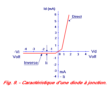
 Click here for the next lesson or in the summary provided for this purpose.
 Top of page
 Next Page