The technique of the diffusion junction consists essentially of exposure to vapors and moderate heating of the semiconductor for the fabrication of these transistors.
By properly choosing the temperature of the semiconductor and using materials in the vapor state, a number of atoms are obtained which diffuse into the crystal lattice of the semiconductor and form an type N or type P zone clearly distinct from the rest of the original semiconductor.
If, initially, the semiconductor is of type P, it is necessary to use in the vapor state materials making it of type N and vice versa.
With this method, it is possible to obtain very thin bases and to adjust their thickness with a remarkable precision by regulating the temperature and the duration of the diffusion process. Moreover, in the bases thus formed, there is always a gradient of concentration of the impurities which thus causes the drifting effect.
By reducing the thickness of the base and simultaneously using the drift effect, we obtain transistors for high and very high frequencies that are used in FM receivers and TVC instead of alloy transistors based on the drift effect. The diffusion method did not, however, completely replace the alloy process. Even now, certain types of high frequency transistors are obtained by a method which combines the alloy and diffusion methods.
In Figure 10, we can see the internal constitution of a transistor manufactured with the mixed diffusion technique and alloy.
These transistors are sometimes designated by the American acronym MADT formed of the initials of the words Micro-Alloy Diffused-base Transistor (micro-alloy transistor with base obtained by diffusion).
Let's see briefly the main phases of the fabrication of these transistors.
Initially, slices obtained from a single crystal of germanium P are available. They are exposed to impurity vapors so as to form a fairly deep N layer. Then each slice is divided into a number of pellets and on each of them are placed two doses of impurity material.
A dose consists of material which, by penetrating into the N layer obtained previously, renders it partially of type P ; the other dose must consist of material which leaves unchanged the fundamental characteristics of the N semiconductor.
By heating the impurity materials to their melting temperature, two alloying processes are formed on the N layer : one relating to the first type of material by which the formation of a layer P on the N layer is obtained. broadcasting ; the other relating to the second type of material by which a single electrical contact is obtained for the external connection of this layer N.
The alloying processes being completed, each chip is cut out and the upper edge is removed. The form illustrated in Figure 10-a is obtained (see the diagram above).
The transistor housing (Figure 10-b) is filled with silicone grease which, as we said earlier, serves to protect the device from chemical agents and mechanical stresses.
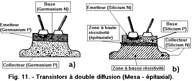
In other types of transistor, the alloy process has been abandoned and the diffusion process is repeated for the formation of the last electrode, that is to say that of the emitter. With this method, the basic structures illustrated in Figure 11 have been obtained.
The section of a mesa-type double-diffusion transistor is shown in Figure 11-a. The name of this transistor comes from the Spanish term "mesa" which means plain or plateau and which is commonly used in America to designate heights typical of the California desert and other regions. These heights are formed by walls more or less steep ending at the top by a fairly large flat surface. The profile of the transistor mesa reminds a little, hence its name.
The structure shown in Figure 11-b also recalls the profile of the mesa but differs from the previous one by the semiconductor used (silicon instead of germanium), by the succession of layers (NPN instead of PNP) and especially by sharing collector in two superimposed zones (high resistivity zone and low resistivity zone).
In general, the collector consists of a single zone having a fairly high and uniform resistivity ; therefore when the collector current is close to or equal to the maximum value, there is a significant voltage drop and power dissipation. But this disadvantage can be mitigated by reducing the resistance of the collector, that is to say by forming the collector with a low resistivity main layer by supplementing it with a high resistivity layer in the contact zone with the base (layer epitaxial).
The axial epitilic layer is obtained by depositing on a semiconductor chip at low resistivity another semiconductor of the same type but much purer. The deposit must be formed very slowly and under temperature conditions such that they allow a normal growth of the crystal on the reticle of the pellet.
By the double diffusion method, the base and emitter are formed leaving free a thin layer forming the collector together with the low resistivity area.
With the described axial epitope technique, transistors are fabricated which are used in the computer multivibration circuits and in other circuits where the transistor is to operate with the maximum collector current.
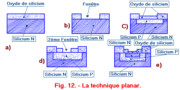
Let us briefly examine, now, a last method of manufacturing transistors with the double diffusion process, that is to say the so-called planar technique.
This technique is a more recent method adopted for the preparation of transistors and it provides only the use of silicon.
As the name implies, the planar transistor is made up of a relatively planar surface obtained by diffusing the base and emitter regions within a silicon wafer which serves as a collector.
For the preparation of a planar silicon transistor, a silicon wafer, which we assume to be N-type, is superficially oxidized (Figure 12-a).
The silicon oxide layer is the key to the planar process. Indeed, this coating serves to protect the material against moisture and dust, which could cause junction instability and therefore cause malfunctions of the transistors. This layer also prevents the diffusion of impurities into the material during the manufacturing process.
On one side of the wafer, part of the silicon oxide is etched away to expose the original semiconductor (Figure 12-b).
Through the window thus formed in the oxide coating, a certain amount of boron is allowed to diffuse into the single crystal of silicon of conductivity N.
Boron is a trivalent element and thus the conductivity base P is obtained. Then the surface is again oxidized, thus closing the window (Figure 12-c).
With the same process, we then practice a new smaller window than the previous (Figure 12-d) and through it, we let spread phosphorus ; the conductivity transmitter N is thus produced. Finally, the surface is again oxidized.
At the end of these operations, three superimposed zones are obtained : one is constituted by the original semiconductor (silicon N), another is formed by the first diffusion (silicon P) and another is created by the second diffusion (N silicon).
With the same method, two windows (smaller than the previous ones) are then applied to the oxide layer for the connection of the base and emitter electrodes.
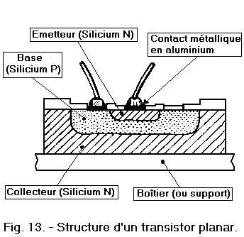
Thus ends the manufacturing cycle of the planar transistor whose basic structure is illustrated in Figure 13.
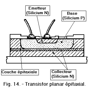
For the preparation of a silicon transistor, it is also possible to use a silicon wafer with an intermediate epitilic layer as for the mesa transistors.
The manufacturing process is similar to that adopted for normal planar transistors.
We can see the structure of an epitaxial planar transistor Figure 14.
Both normal and epitaxial planar transistors have excellent high frequency response with optimum thermal stability characteristics, high efficiency and high reliability of operation.
Their fundamental characteristics are similar to those of the mesa transistors ; however, they have the ability to control higher powers and have much lower leakage currents.
With the planar technique, it is possible to simultaneously obtain a large number of transistors (two thousand and more depending on the diameter of the starting silicon wafer).
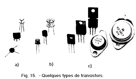
The aspect that presents the transistors is very varied, as well for the shapes of the case as for the dimensions.
The most common types of transistors are illustrated in Figure 15 : high and ultra-high frequencies (Figure 15-a), low frequencies and low power (Figure 15-b). On the other hand, some examples of high-power transistors used at low frequencies, with metal or plastic casings, are represented in Figure 15-c.
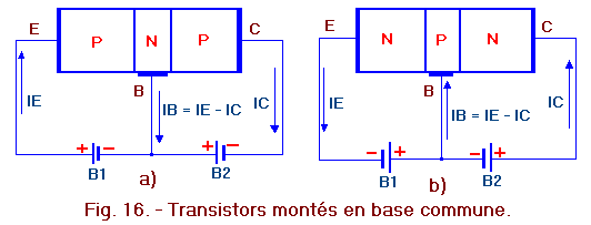
By analyzing the operating principle of the common base transistor, we have seen that the collector current can be controlled by means of the emitter current.
For the transistor to work in this way, it must polarize its direct emitter-base junction and the reverse collector-base by using two separate cells as shown in Figure 16-a in the case of the PNP transistor or as shown in Figure 16-a in Figure 16-b the case of the NPN transistor.
By observing these circuits, it can be seen that the electrode of the base is common to the collector and emitter circuits. Indeed, considering the transistor as a simple device having three terminals, it can be seen that the collector current IC (in the case of the NPN transistor of Figure 16-b), supplied by the wafer B2, flows through the collector electrode, enters the manifold and must exit through the base electrode to return to the negative pole of this battery. Similarly, considering the transmitter circuit, we see how the emitter current supplied by the battery B1 enters the transistor by the electrode of the base and leaves that of the transmitter.
The base electrode is therefore traversed by the collector current IC and the emitter IE ; since these two currents circulate in opposite directions in this electrode, the actual base current is given by their difference and is very low (IC being of little less than IE).
This way of wiring the transistor is called a common base arrangement because the base electrode is common to the emitter circuit comprising the stack B1 as the collector circuit including the stack B2.
Usually, with this type of mounting, the base is connected to ground, it is said that the transistor is mounted with the base to ground.
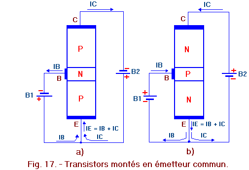
The transistor can also be mounted in a different manner as shown in Figure 17-a in the case of the PNP type or as illustrated in Figure 17-b in the case of the NPN type.
In this new arrangement also, the emitter-base junction is forward biased by means of the stack B1 and the collector-base junction is reverse biased by means of the stack B2 which, this time, is no longer connected between the collector and the base, but between the collector and the transmitter.
The emitter electrode is therefore common to the basic and collector circuits. It is covered by the base current and the collector current as shown in Figure 17.
The total current in the transmitter is given by the sum of the two currents IC and IB ; these circulating in the same direction, so we have IE = IC + IB.
By analogy with the preceding circuit, the assembly of Figure 17 is called a common emitter or emitter-to-ground assembly, since in this case the emitter is common to the input circuit (which is now the basic one instead of the one of the input circuit emitter) and the output circuit (which is still that of collector).
The operation of the common emitter transistor is different from that of the common base transistor because now the collector current is controlled by the base current.
There is a third type of transistor mounting : the common collector or ground collector assembly with which the input circuit is still the base circuit and the output circuit the emitter circuit.
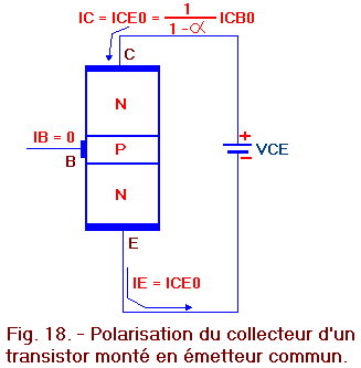
4. 1. - POLARIZATION OF THE COLLECTOR
In the common emitter assembly, the collector voltage is applied between the collector and the emitter with polarities such that the collector-base junction is reverse biased.
So if we consider an NPN transistor, the positive pole of the battery is connected to the collector as shown in Figure 18.
In the circuit, a collector current is circulated which is called ICE0 to indicate that this current is the current flowing between the collector and the emitter when the base current is zero (indeed, the base is not connected and therefore, on its terminal no current flows).
This collector current is similar to the current ICB0 that we saw in the common base assembly.
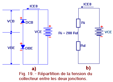
However, ICE0 is much larger than ICB0. To understand this, it is necessary to consider how the voltage VCE of the stack is distributed between the two junctions being in series.
Imagine that the transistor is replaced by two junction diodes (Figure 19-a). One, designated DCB, represents the collector-base junction and the other, designated by DBE, represents the base-emitter junction.
These diodes, as seen in Figure 19-a, are connected in series and are arranged in opposite directions.
The collector-base junction is traversed by the current ICE0 in the NP direction, while the base-emitter junction is traversed in the PN direction.
More precisely, the diode DCB is reverse biased while the diode DBE is forward biased.
The voltage VCE is then divided into two, that is to say a voltage VCB across the diode DCB and a voltage VBE across the diode DBE.
To determine the order of magnitude of these two voltages, it is also possible to replace the two diodes by their internal resistance which, in this circuit, have very different values. Indeed, the diode DCB being reverse biased, has a very high inverse resistance Ri, while the diode DBE being forward biased has a direct resistance Rd of very low value.
In the equivalent diagram illustrated in Figure 19-b, Ri and Rd thus behave as a divider bridge.
Since both resistors are traversed by the same current ICE0, the voltage across each of them is directly proportional to the value of these resistors, therefore the value of the voltage VCB is significantly greater than that of the voltage VBE.
To take an example, we can assume that Rd is 200 times smaller than Ri. The voltage VBE at the terminals of Rd will then be 200 times smaller than the voltage VCB across Ri.
(We report the same diagram above to make reading easier, see Figure 19).
It can thus be seen that the battery voltage is not fully applied to the collector-base junction, but that a small portion of this voltage is located across the base-emitter junction so as to bias it directly. There is therefore on the part of the transmitter, emission of a certain quantity of electrons which diffuse in the base and which reach largely the collector.
The collector current will not be only the current ICB0, but also the current due to the emission of electrons from the transmitter.
To know the expression of ICE0 as a function of ICB0, it suffices to use the formula already seen in the common base assembly, that is to say IC = IE +ICB0.
In this case, IC = IE = ICE0. It follows that :
ICE0 = ICE0 + ICB0
ICE0 (1-) = ICB0
is ICE0 = 1/(1-)
x ICB0
To get an idea of the ratio that exists between ICE0 and ICB0, suppose that is equal to 0.98 and that ICB0 is worth 5 µA.ICE0 = 250 µA is thus obtained, that is to say that ICE0 is 50 times greater than the current ICB0 obtained with the same transistor mounted in a common base.
The value 1 / (1 - ) obviously depends on the value of the transistor considered and is even larger than is close to 1.
The ICB0 and ICE0 values reported previously are given for information only and relate to germanium transistors.
In the case of silicon transistors on the other hand, the current ICB0 is generally a thousand times smaller and the current ICE0 remains negligible although being given by the same formula.
4. 2. - BASE POLARIZATION AND AMPLIFIER COEFFICIENT
In the common transmitter arrangement, the input circuit current is the base current IB and the output circuit current is the collector current IC.
By increasing the bias voltage VBE of the base, the base current IB is increased and the collector current IC is proportionally increased. In other words, the current IC is controlled by the current IB.
The ratio between the collector current IC (reduced by the residual current ICE0) and the base current IB can thus be defined as current amplification coefficient. This coefficient called beta (second letter of the Greek alphabet whose symbol is ) is given by the formula :
= IC - ICE0 / IB
In practice however, the value of ICE0 is very low compared to IC, therefore negligible.
The value of the coefficient can be determined by the simple ratio between IC and IB and we can write :
= IC / IB
To get an idea of the value of the coefficient presented by the transistors, it should be remembered that the base current IB is given by the difference between IE and IC and that the emitter current IE is little greater than the collector current IC.
It is deduced that the basic current IB must have a very small value with respect to IC.
The values of must therefore be very large and no less than 1, as is the case for the coefficients . Let's say according to
in terms of .
We know that :
IC =
IE + ICB0.
=
IE + (1 - )
ICE0
=
(IB + IC) + (1 - )
ICE0
from where
IC (1 - )
=
IB + (1 -
)
ICE0
(1 - )
(IC - ICE0) =
IB
is
IC - ICE0 / IB =
/ (1 -
)
from where
=
/ (
- 1)
This formula therefore makes it possible to calculate the amplification coefficient when we know the amplification coefficient .
For example for a transistor that has a coefficient
= 0,98 we will have, with the common transmitter assembly, a coefficient of amplification
equal to :
= 0,98 / (1 - 0,98) = 0,98 / 0,02 = 49
So we see that , in contrast to , is much larger than 1. This explains the great difference that exists between the two types of mounts (see, Common Base and Common Transmitter).
In the case of the common emitter assembly, only a small base current is required to cause a significant increase in the collector current. In fact, the collector current, which in the absence of polarization of the base (IB = 0), has the value ICE0 (residual current), increases by a value equal to the value of the current that is made circulate in the base.
The collector current is given by the formula IC = IB + ICE0, see neglecting ICE0 : IC = IB.
The values that are encountered in practice for low and medium power transistors, such as those used in radio receivers, range from 20 to 600 depending on the type.
It is important to note that the amplification coefficients and are only related to the static operation (in direct current) of the two circuits considered (respectively common base and common emitter).
If a signal is applied to the input of the two circuits, these two amplification coefficients are designated by another symbol and take different values.
4. 3. - COMPARISON BETWEEN THE TWO TYPES OF ASSEMBLIES :
We have seen that the transistor has a greater current gain in the case of the common emitter than in the common base assembly and that a high collector current with a relatively low base current is obtained.
To fix ideas, we can notice that a low frequency preamplifier transistor mounted as a common emitter has a base input current of the order of a few tens of microamperes, while for the same transistor mounted in common base, the input current (emitter) is of the order of a few milliamperes.
Consider now the power gain, which is defined by the ratio of the power supplied in the collector circuit and that supplied in the circuit of the base.
The power gain is greater for a common emitter than for a common base but the residual current is higher in the first assembly.
In the diagrams given so far, the transistor has always been represented by means of three rectangles symbolizing the three semiconductor zones of which it is constituted.
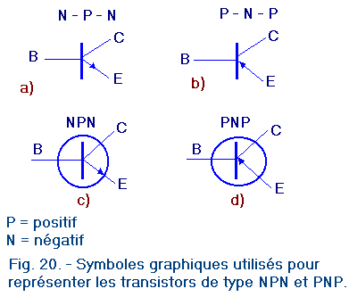
In the circuit diagrams of transistor devices, however, it is customary to represent the transistor by a graphic symbol also indicating, in a conventional manner, the type of the transistor, that is to say whether it is NPN or PNP.
Among the many graphic symbols used in the past, those shown in Figure 20 have gradually become widespread.
In these symbols, the thick vertical line represents the semiconductor regions from which the three electrodes depart.
On the left side, the small horizontal line represents the base electrode; on the right side, the two small inclined lines represent the emitter and collector electrodes.
To differentiate the transmitter from the collector, on the first one draws an arrow whose direction also has the role of indicating whether it is an N transistor or a PNP transistor.
The choice of direction of the arrow has been made so that it indicates the direction in which the direct current of the base-emitter junction flows.
Thus, remembering that a junction leads in the direction, it is easy to establish that the arrow is outwardly oriented (see from the P-type base to the N-type transmitter) in the case of the NPN transistor, while in the case of the PNP transistor, this arrow is directed inward (see from the P-type transmitter to the N-type base).
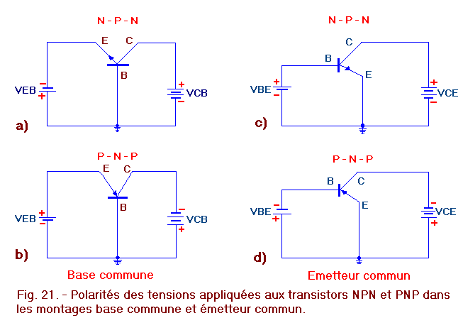
To recall the polarities of the voltages to be applied to the transistors in the case of the common base and common emitter assemblies for the NPN type as for the PNP type, the diagrams relating to the four possible cases have been gathered in Figure 21.
a)- common base-NPN transistor assembly (Figure 21-a) :
VCB collector voltage : positive
Transmitter voltage VEB : negative
b) - common base assembly - PNP transistor (Figure. 21-b) :
collector voltage VCB : negative
Transmitter voltage VEB :positive
c) - NPN common transistor emitter assembly (Figure 21-c) :
Collector voltage VCE : positive
basic voltage VBE : positive
d) - PNP common transistor emitter assembly (Figure 21-d) :
collector voltage VCE :negative
basic voltage VBE :negative
From these diagrams, it can be noted that the collector voltage is always positive in the case of NPN transistors and negative in the case of PNP transistors while the voltage of the control electrode (transmitter and base respectively in the two types mounting) is of opposite polarity to that of the collector in the common base assembly and is of the same polarity as that of the collector in the common emitter assembly.
In the next lesson, we will examine the sequence of transistors and the continuity of the assemblies in this lesson, but with other related components. (Semiconductors 5).


 Fundamental montages of transistors
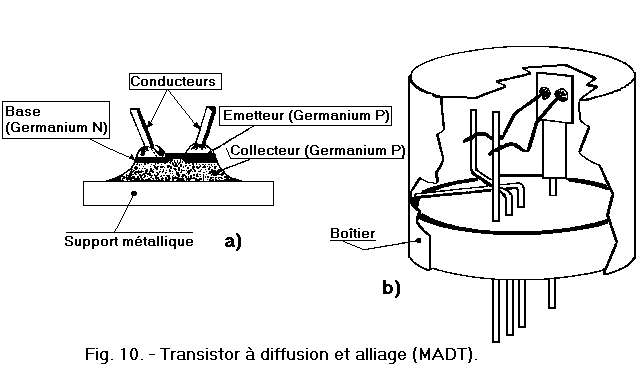
 Click here for the next lesson or in the summary provided for this purpose.
 Top of page
 Next Page
