This lesson follows the transistor review begun in previous lessons.
The first chapter will be devoted to the examination of the characteristic curves of the transistor.
The second chapter will indicate the use that we make of these characteristic curves. Finally, the last chapter will be devoted to the effect of temperature on the operation of the transistor.
1. - CHARACTERISTIC CURVES OF THE TRANSISTOR
1. 1. -CURVES AND CHARACTERISTIC NETWORKS OF THE TRANSISTOR
You have seen that the characteristic curve of the diode makes it possible to know its operation. Indeed, for each voltage applied across the diode, the characteristic allows to know the current flowing through it.
It is the same for the transistor ; that is, its properties can be determined by characteristic curves.
Nevertheless, the case of the transistor is different from that of the diode. Firstly, it can be used in the three basic arrangements (common emitter, common collector, common base) and therefore, the characteristic curves will depend on the particular assembly examined.
Then, the transistor has four electrical quantities while the diode has only two. This is clear in Figure 1.
These four electrical quantities are the two voltages Ve and Vs, and the two currents Ie and Is.
The voltage Ve, applied between the control electrode and the common electrode and the current Ie flowing through the control electrode define the input circuit of the transistor.
In the same way, the voltage Vs, applied between the output electrode and the common electrode, and the current Is flowing in the output electrode define the output circuit of the transistor.
A characteristic curve represents the relationship between two electrical quantities. In this case, there are four electrical magnitudes. It is therefore possible to draw six characteristic curves (Ve - Ie, Vs - Is, Ve - Is, Vs - Ie, Ve - Vs, Ie - Is).
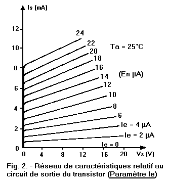
In addition, the four electrical quantities are all dependent on each other. Consequently, for a given pair of magnitudes, there are several characteristics that are called a characteristic network. Take the example of the pair Vs - Is. You know that the current Is is a function of the current Ie (Is is also a function of the voltage Ve since it determines Ie).
Therefore, it is possible to draw a characteristic curve for each value of the current Ie.
Ie is the parameter relating to the characteristic network Vs-Is. Figure 2 represents the characteristic network relating to the pair Vs-Is (output characteristic network).
For each of the six couples listed above, there is a network of characteristics that is plotted against a parameter. Thus, it is possible to draw the characteristic network relating to the pair Ve - Ie having for parameter Vs (input characteristics). We will return to this example later.
So far, we have matched a single parameter for a given pair of electrical quantities (for example the parameter Ie for the pair Vs - Is).
However, it is possible to match a second parameter for each of the six aforementioned couples. This is explained by the fact that there are four electrical magnitudes. For example, for the output characteristics (pair Vs - Is), the parameter can be Ve. In this case, for each particular value of Ve, there will be a characteristic curve. Thus, it is possible to plot 12 (6 x 2) networks of different characteristics.
However, to know the properties of a transistor, it suffices to have two networks of characteristics. The other ten are graphically deduced.
We will discuss in this chapter networks of characteristics usually provided by manufacturers in technical documentation.
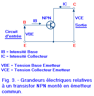
In addition, we will consider the common transmitter assembly because we saw that it had many advantages over the common base.
The electrical quantities used appear in Figure 3.
The input circuit is defined by the VBE voltage (Transmitter Base Voltage) and the current IB.
The output circuit is defined by the voltage VCE (Emitter Collector Voltage) and the current IC.
1. 2. - CHARACTERISTIC CURVES RELATING TO THE COMMON TRANSMITTER MOUNTING OF AN NPN SILICON TRANSISTOR :
1. 2. 1. -REVIEWING THE OUTPUT CIRCUIT
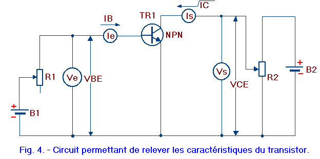
In order to draw these curves, it is necessary to carry out the assembly of Figure 4. (See below).
The latter comprises four measuring devices and two DC power supplies B1 and B2.
The battery B1 makes it possible to directly polarize the base-emitter junction. The variable resistor R1 makes it possible to vary the base current IB.
is a millivoltmeter and is used to measure the input voltage VBE, while the base current IB is measured by the microampereimer .
The B2 cell polarizes in reverse the collector-base junction. Resistor R2 makes it possible to vary the voltage VCE. This voltage VCE is measured with the voltmeter ,
while the output current IC is measured with the milliammeter .
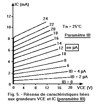
We will now proceed to draw the characteristic network relating to the torque VCE / IC electrical quantities using as parameter the basic current IB.
This network of features, which is one of the most used, is shown in Figure 5.
The voltage VCE is carried on the horizontal axis of the Cartesian coordinate system, while the current IC is carried on the vertical axis.
To plot the characteristic relating to IB = 0, simply open the input circuit (the base is in the air). Then, VCE is varied using resistor R2 ; For example, volts in volts (0, 1, 2, 3 ... volts). For each value of VCE, the value of the corresponding current IC is measured. You notice that the characteristic for IB = 0 is practically merged with the horizontal axis. There is a very low ICEO current which is a leakage current.
Then, to trace the second characteristic (IB = 2 µA), the input circuit is closed and R1 is set so that the current IB is equal to 2 µA. It is then sufficient to make a series of measurements as previously by acting on R2, which makes it possible to trace the second characteristic.
Then we go to the third characteristic for IB = 4 µA and so on ...
In the present case, the network comprises 13 characteristics and IB varies from 0 to 24 µA.
We will detail the review of this network.
All the characteristics start from the origin point 0. This means that when VCE is zero, the current IC is also zero and this whatever the current IB.
Then, the features have two parts. The first is common and practically vertical ; the second is practically horizontal and is a function of the current IB.
The first part means that when the voltage VCE varies slightly, the current IC increases in significant proportions and especially as the current IB is high.
When the voltage VCE reaches a certain threshold, relatively low for each characteristic, there is a bend and at this point the curve becomes practically horizontal. In fact, it is slightly raised, that is to say that for each value of IB given, the current IC increases slightly when the voltage VCE increases.
The position of a characteristic is here a function of the current IB, in other words the current IC is in close relation with the current IB.
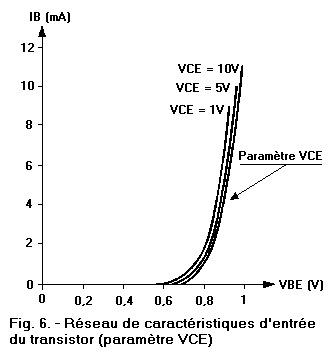
1. 2. 2. - REVIEW OF THE INPUT CIRCUIT
The characteristic network relating to the input circuit (quantities VBE and IB) is determined by means of the assembly located in Figure 4, (diagram shown below) with a procedure different from the previous one. The micro-ammeter
is replaced by a milliammeter.
In a first step, the voltage VCE is fixed using the resistor R2.
In a second step, we note the characteristic for different values of IB. For this, R1 is varied and for each value of IB, the voltage VBE is read. This determines a characteristic. For a second characteristic, the value of VCE is changed and the same series of measurements is repeated. Several characteristics are thus drawn as shown in Figure 6.
You notice immediately that these characteristics are similar to that of a diode. Indeed, the base-emitter junction is forward biased.
However, when IB is zero (base in the air), the voltage VBE is not zero, but is worth about 0.6 volts.
You also note that the voltage VCE has very little influence on the voltage VBE. If for the same basic current VCE goes from 1 volt to 10 volts,the voltage VBE varies only a few tens of mV.
As a result, the manufacturers merely provide a single input characteristic, corresponding to an average value of VCE.
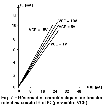
1. 2. 3. - CHARACTERISTICS NETWORK RELATING TO IC AND IB SIZES (VCE PARAMETER)
The assembly used is always that shown in Figure 4 above.
In a first step, the voltage VCE is fixed using R2. Then in a second step, R1 is set so as to vary the current IB. It is sufficient to record the value of the current IC for each particular value of the current IB.
The network of Figure 7 is thus obtained.
These characteristics are called transfer characteristics because they relate the IC output current to the input current IB.
You notice that IC is proportional to IB (to constant VCE).
More than VCE is high, the coefficient of proportionality between IC and IB is high.
In reality, transfer characteristics are not exactly straight lines, but practically we can equate them with straight lines
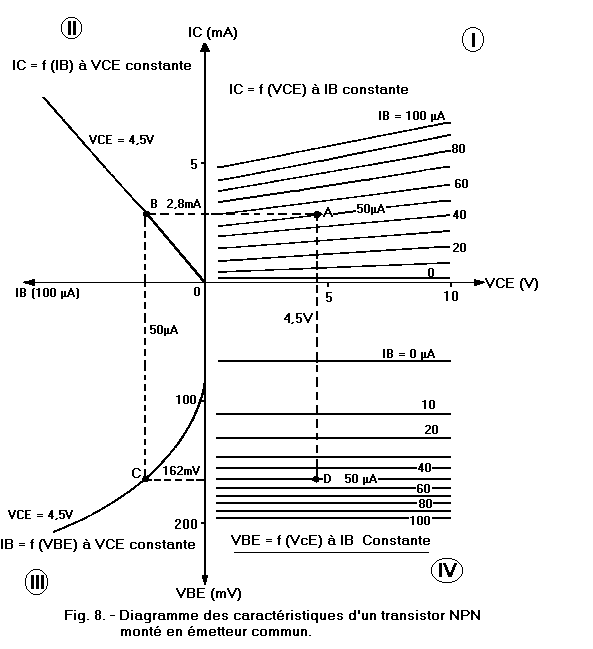
1. 2. 4. - GENERAL DIAGRAM OF THE CHARACTERISTICS OF A TRANSISTOR
It is possible to bring together the three networks of features previously seen.
This grouping is shown in Figure 8.
There are four quadrants.
The output characteristics are arranged in the quadrant (I) located at the top and on the right.
Quadrant II at the top left is a transfer feature. Compared to Figure 7, the increasing IB currents are counted to the left of the origin 0.
Finally, quadrant III represents an input feature.
In quadrant IV, we represent the network of characteristics relating to the reaction of the output circuit on the input circuit.
In the case of common transmitter mounting, these characteristic networks give the following values :
Quadrant I : Output characteristics. The value of the output current IC is determined as a function of the output voltage VCE at constant basic current. We write : IC = f (VCE) to IB = constant.
Quadrant II: Transfer characteristics. Used to find the IC output current according to the input current IB, at constant output voltage VCE. We write : IC = f (IB) to VCE = constant.
Quadrant III :Input Features. Here the value of the input current IB is obtained as a function of the VBE input voltage at the output voltage VCE = constant. We write : IB = f (VBE) to VCE = constant.
Quadrant IV:Reaction characteristics.These characteristics make it possible to determine the reaction ratio, that is to say the influence of the output voltage VCE on the input voltage VBE, at constant base current IB. We write : VBE = f (VCE) to IB = constant.
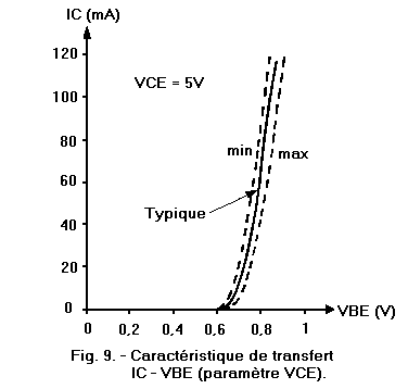
A constructor can provide other characteristics than those already seen so far. In particular, the characteristic relating to the current IC and to the voltage VBE can be given (Figure 9). The voltage VCE can be constant.
Since there is a dispersion related to the fabrication of the transistors, the manufacturer indicates a typical characteristic as well as the minimum characteristic and the maximum characteristic.
The majority of transistors, however, have characteristics that substantially coincide with the typical characteristic.
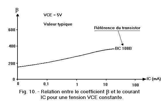
Another characteristic indicating the variation of the coefficient as a function of the current IC can be provided by the manufacturer (Figure 10).
This characteristic does not belong to the group of the 12 networks of characteristics mentioned above.


 Footer
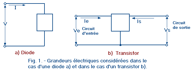
 Click here for the next lesson or in the summary provided for this purpose.
 Top of page
 Next Page