2. - USE OF THE CHARACTERISTIC CURVES OF A TRANSISTOR
2. 1. - DETERMINING AN OPERATING POINT
The characteristics of the transistors are used to determine the operating conditions of these transistors.
The value of the electrical quantities involved in this operation is thus determined.
The most used feature is the one that relates to the output circuit.
Consider the feature network of Figure 11.
That is a voltage VCE equal to 10 volts and a current IB equal to 70 µA.
To determine the current IC corresponding to these two given parameters, it is sufficient to draw a vertical from the voltage VCE = 10 V ; this vertical crosses the characteristic relative to IB = 70 µA at point A. From this point A, it is necessary to draw a horizontal line which intersects the vertical axis of the Cartesian coordinate system. In the present case, IC = 20 mA is found.
Point A is called the operating point. Indeed, this point A makes it possible to know the three parameters relating to the operation of the transistor.
You notice that you only need to know two of three parameters to determine this operating point.
Suppose for example that we know IC = 14 mA and IB = 50 µA.
Just draw a horizontal line corresponding to IC = 14 mA ; this meets the characteristic IB = 50 µA at point B. The vertical trace from point B is then drawn, which makes it possible to determine a voltage VCE equal to 9 volts.
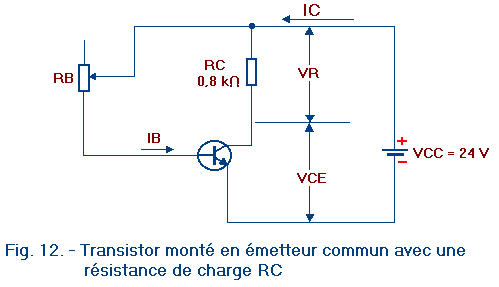
We will now examine the operation of the assembly located in Figure 12.
The common transmitter assembly is powered by a 24 volts battery. The variable resistor RB makes it possible to vary the basic current IB.
The resistor RC is the load resistor located in the collector of the transistor.
The voltage across the load resistor is VR. The sum of the voltages VR and VCE is equal to VCC is 24 volts.
We want to know the relationship between the three variables VCE, IC and IB. For example, we have the output characteristics network with parameter IB.
It is enough to choose a certain number of values for the current IC, then to calculate the voltage VCE for each of these values. This will allow us to place as many points on the feature network.
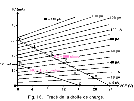
For IC = 5 mA,
VR = RC x IC = 800 x 5 x 10-3 = 4 volts, soit VCE = VCC - VR
from where VCE = 24 - 4 = 20 volts.
This gives us the coordinates of a first point which we call A in figure 13.
In the same way, for
IC = 10 mA, VR = 8 volts and
VCE = 16 volts (point B).
For IC = 15 mA, VCE = 12 volts (point C)
For IC = 20 mA, VCE = 8 volts (point D)
For IC = 25 mA, VCE = 4 volts (point E)
You notice that these five points are aligned ; also, we can pass a line by these points that we call charge line.
This load line represents the set of operating points for the transistor. That is to say that for each point of the line, one can determine the three quantities VCE, IC and IB corresponding.
This line meets the two axes of the marker at the points P and Q. The point Q corresponds to a voltage VCE of 24 volts and a current IC zero. The point P corresponds to IC = 30 mA and VCE = 0 volts ; in this case, the voltage VR is equal to the voltage VCC.
As you know, you only need to know two points to determine a line. Now, in this case, it is possible to know these two points to draw the load line.
We will take an example. Let a load resistor RC equal to 1.3 KΩ and a supply voltage VCC equal to 16 volts.
When IC is zero, we know that VR = 0 volts and VCE = VCC = 16 volts. We have therefore determined the point Q' on the horizontal axis (Figure 13). To determine the second point, we set VCE = 0 volts. In this case VR = 16 volts and IC = VR / RC = 16 / 1.3 x 103 = 12.3 mA.
The second point P' therefore corresponds to IC = 12.3 mA. (Application of Ohm's Law).
It remains to connect these two points P' and Q' and thus, one has drawn the right of charge relative to RC = 1.3 KΩ and VCC = 16 volts.
Its position is clearly different from the one examined previously.
These two examples therefore demonstrate that the position of the load line is a function of VCC and RC.
It is not always possible to determine the two points on the two axes of the marker.
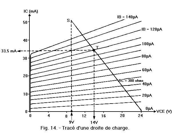
Take the case of the network in Figure 14.
Is VCC = 24 volts et RC = 0,3 kΩ.
When IC = 0 mA, VCE = VCC = 24 volts. We therefore know the point Q located on the horizontal axis.
For VCE = 0 volt, We have IC = VR / RC = VCC / RC is
IC = 24 / 300 = 80 mA.
However, the point corresponding to IC = 80 mA is located outside the graph, so it is necessary to look for another point.
We therefore take IC = 50 mA.
We deduce VR = RC x IC = 300 x 50 x 10-3 = 15 volts
and VCE = VCC - VR = 24 - 15 = 9 volts.
Thus, the second point S corresponds to VCE = 9 volts and IC = 50 mA.
The load line is therefore determined by the points Q and S.
Therefore, it is easy to determine the values of the VCE and IC quantities if the current IB is set.
For example, the characteristic corresponding to IB = 110 µA meets the load line at point T (Figure 14).
This point makes it possible to know VCE = 14 volts and IC = 33.5 mA.
2. 2. - LIMIT VALUES FOR A TRANSISTOR
Like any component, the transistor can only operate between certain limit values of the electrical quantities linked to it.
These limit values are related to the type of transistor, its dimensions, its constitution ...
For example, a small transistor will dissipate less power than another of larger dimensions.
For each type of transistor, the manufacturer supplies limit values that must not be exceeded under normal conditions of use. Otherwise, the transistor may be irreparably damaged, or at least cause abnormal operation.
The limit values generally provided by the manufacturers are as follows :
Maximum collector current IC max.
The maximum collector voltage VCE max.
Maximum power of PC collector max.
The maximum temperature of the junction Tj max.
Other limit values for the base and the transmitter can be provided.
a) The maximum value of the collector current
This value is determined so that the transistor operates properly and so that the junction can not be damaged.
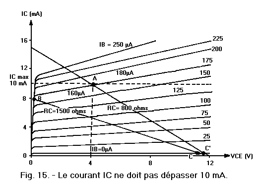
In Figure 15, this limit value IC max is represented by a horizontal dashed line. In this case, IC max = 10 mA.
The operating point of the transistor must be below this dotted line.
Depending on the value of the RC resistor, two situations are to be considered.
In the first case, the load line is entirely below the dotted line. This is the case, for example if RC = 1.5 kΩ (Figure 15).
All operating points are thus located below this dotted line.
In a second case (RC = 800 ohms), the charge line intersects the dotted line, for example at point A in the example of Figure 15. In this case, it is necessary to limit the current IB to 180 µA. Indeed, the characteristic relating to IB = 180 µA passes precisely through this point A and any operating point of the transistor can not be chosen above the point A. It can be said that A is a limit point for the operation of the transistor.
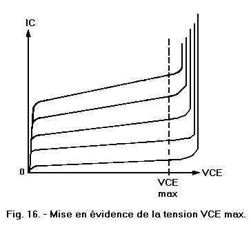
b) The maximum value of the collector voltage
During the examination of the diode junction, you saw that there was a reverse voltage called "breakdown voltage" beyond which the diode was damaged. However, in the transistor, the collector-base junction is equivalent to a reverse biased diode.
There is therefore a maximum voltage between the collector and the base of the transistor not to be exceeded. In other words, there is a voltage VCE max.
In Figure 16, the voltage VCE max is indicated by the dotted line.
The operating point of the transistor should be located to the left of this dotted line.
If the voltage VCE significantly exceeds the value of VCE max, IC becomes very important and the transistor may be destroyed.
c) The maximum value of the dissipation power of the collector
The transistor absorbs a power equal to the product of the voltage VCE by the current IC.
We have the relationship :
PCwill be expressed in mW, if VCE is in volts and IC in mA.
This power absorbed by the transistor corresponds to a consumption of electrical energy.
This electrical energy is converted in the transistor into heat energy by Joule effect. Therefore, there is heating of the transistor ; in particular the temperature of the junction increases.
However, as the junction temperature can not exceed a certain value, it is necessary to limit the power dissipated by the transistor.
The increase of the temperature of the junction can be deduced from the following formula :
T'j is the temperature increase indicated in °C.
Rth is a coefficient called thermal resistance of the transistor, depending on the type of transistor.
Pc is the power absorbed by the transistor.
The coefficient Rth is expressed in °C / W and indicates the increase in temperature of the junction in °C
for a power dissipation of one watt.
Let's take an example :
Rth = 400°C / W, VCE = 5 volts, IC = 3 mA,
PC = 5 x 3 = 15 mW
From where
T'j = 400 x 0,015
= 6° C
The temperature of the junction increases by 6° C.
To calculate the temperature of the junction, it is necessary to apply the relation :
Tj = Ta + T'j
(2)
Tj is the temperature of the junction.
Ta is the ambient temperature.
Taking the example above with Ta = 25°C, we have :
Tj = 25 + 6 = 31° C
The maximum permissible temperature at the junction is between 150° C and 200° C for a silicon transistor.
The temperature of the junction Tj depends on the ambient temperature Ta and the temperature increase T'j which is a function of PC. Therefore, the maximum permissible power PC max depends not only on the type of transistor but also on the Ta.
A constructor therefore indicates a value of PC max for a temperature Ta fixed.
Generally, the values of Rth and Tj max are provided by the manufacturer.
Under these conditions, one can calculate PC max from relations (1) and (2) :
If we know the values of Tj max, Ta and Rth, it is easy to calculate PC max.
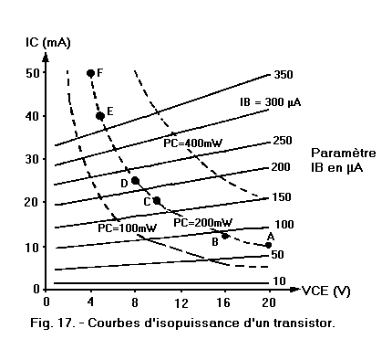
It is interesting to see how the knowledge of PC max limits the area of use of the feature network.
Since the value of PC max is known, it is easy to draw a curve representing the relation.
VCE x IC = PC max
Figure 17 represents an example with three curves relating to three values of PC max
(400 mW, 200 mW and 100 mW).
These curves are called isopower curves, because for all the operating points located on a curve, the power dissipated by the transistor is identical.
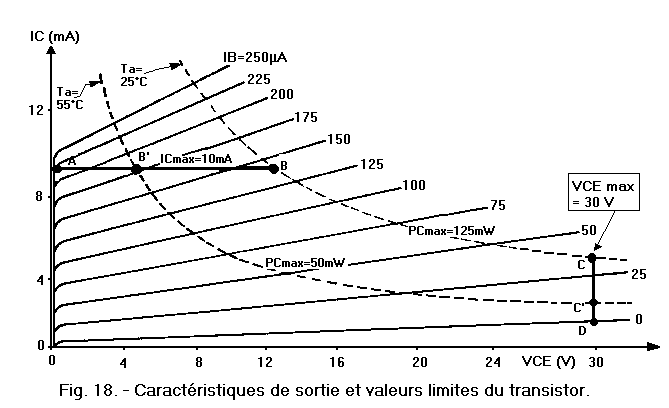
Generally, the isopower curve, IC max and VCE max are reported on the characteristics network as shown in Figure 18.
Any operating point must be located in the area between the two axes of the marker, the two line segments representing IC max and VCE max and the isopower curve corresponding to the transistor used.
For an ambient temperature of 25° C, PC max is equal to 125 mW and therefore the useful area is delimited by the points 0, A, B, C and D.
This useful area decreases rapidly if the ambient temperature increases : If Ta = 55° C, PC max = 50 mW ; in this case, the useful area is delimited by the points 0, A, B', C' and D.


 Footer
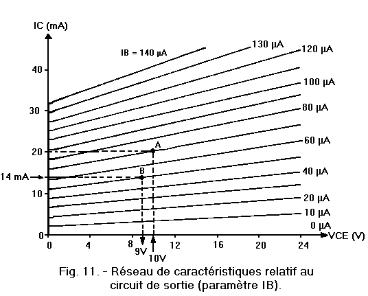

 Click here for the next lesson or in the summary provided for this purpose.
 Top of page
 Next Page