FIELD EFFECT transistors are designated by the abbreviation F.E.T. (Fild Effect transistor).
The transistors F.E.T. completely different from the types studied so far, so much so that even the electrodes have a special name. In fact, when it is a normal transistor, the emitter corresponds to the electrode from which the charge flow (electrons or holes) starts, the collector the electrode collecting this flux and the BASE electrode for controlling it.
In a transistor F.E.T. the electrode from which the charge flow is emitted is called SOURCE, the electrode receiving this flow is called DRAIN and finally, the electrode for controlling the flow is called DOOR.
Figure 1 represents the schematic structure of a F.E.T.
This device consists of a silicon block into which impurities have been introduced, so as to obtain a type N semiconductor.
Two conductive plates are applied to the ends of this block, one of which represents the SOURCE and the other the DRAIN.
On the sides of the block, two P-type zones are formed, constituting the DOOR (Figure 1). Thus, between these two P-type zones, an N-type channel extends from SOURCE to DRAIN.
The block thus comprises two P.N. junctions.
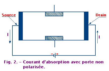
Suppose that a voltage is applied between the SOURCE and the DRAIN, by means of a battery connected between these two electrodes (figure 2).
The door remains free for now.
Under these conditions, the silicon block behaves as we saw earlier by treating conduction problems in an N-type semiconductor.
The MAJORITY CARRIERS (electrons), go from the SOURCE (negative) to the DRAIN (positive), creating in the external circuit an ABSORPTION CURRENT which according to the conventional sense, is directed in the direction of the arrow shown in figure 2.
The intensity of this current depends on the resistance that the electrons encounter along the channel, from the SOURCE to the DRAIN. Thus, decreasing the width of the channel increases resistance as the section is smaller.
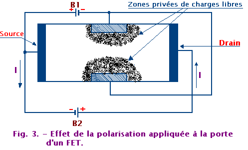
It is possible, electrically, to reduce the current that is to say to increase the resistance of the channel, POLARIZING THE DOOR IN THE REVERSE DIRECTION, compared to the SOURCE. For this purpose, simply connect a battery between the two areas P, as shown in Figure 3.
Note that the two P-type zones constituting the door, are connected directly to each other and connected to the negative of the battery B1. The positive of this same battery is connected to the SOURCE (Figure 3).
Under the effect of the inverse polarization, a zone deprived of free charges is formed near the junctions, THEREFORE A ZONE WHERE THE CURRENT CAN NOT CIRCULATE. Figure 3 illustrates this phenomenon. Indeed, the narrowing of the channel leads to an increase in resistance, the increase of which results in reducing the intensity of the absorption current.
Since the amplitude of the zones deprived of free charges depends on the value of the polarization voltage of the DOOR, it is understood that WHEN THIS VOLTAGE VARIES, THE INTENSITY OF THE ABSORPTION CURRENT IS ALSO VARYING.
It is even possible, by increasing the reverse bias voltage, to completely BLOCK THE CHANNEL, that is to say to completely interrupt the flow of the absorption current.
The value of the voltage for which this phenomenon occurs is called PROHIBITION VOLTAGE. Thus, the transistors F.E.T. allow to control a current by means of a tension. This current control does not require any power expenditure. Indeed, the control voltage being applied between the DOOR and the SOURCE, (so as to polarize in the opposite direction the junction located between the two zones P and the zone N) gives rise to only the passage of the INVERSE CURRENT, very low.
In this way, the INPUT RESISTANCE of transistors F.E.T. reaches values of the order of 10 000 MΩ, values much higher than those of current transistors. Thus, F.E.T. thus, the properties of ordinary transistors have the advantage of having a high resistance.
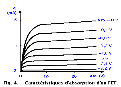
For these components, it is obviously possible to note the characteristic curves, among which the family of absorption characteristics, having for parameter the voltage VPS (voltage applied between the DOOR and the SOURCE) we are particularly interested.
Apply a VPS voltage of determined value between the DOOR and the SOURCE and vary the voltage V.A.S. (voltage present between the drain and the source) and for each value of it, measure the absorption current IA.
The data needed to plot a first absorption characteristic on a Cartesian diagram are thus found. It is also possible to obtain other characteristics by giving various values to the voltage VPS and finding for each of them the values taken by the current IA, when the voltage V.A.S. varied.
Figure 4 gives an example of a family of absorption current characteristics as shown in Figure 3.
It is particularly noted that from a certain point, the absorption current IA does not increase substantially, even if the voltage VAS continues to grow.
We note indeed that the zones deprived of free loads, do not have a constant extension along the DOOR, but on the other hand, these are much wider on the side of the DRAIN.
This division of the zones is due to the fact that the voltage present between the DOOR and the SOURCE increases as it approaches the DRAIN, because of the voltage drop occurring along the channel, under the effect of current flowing from SOURCE to DRAIN.
However, as we have seen, the increase in this area reduces the channel that is to say increases the resistance, which reduces the current.
It is thus understood that the absorption current can not increase indefinitely, because from a certain value, its increase determines a narrowing of the channel, limiting the intensity of this current.
The structure of F.E.T. shown in Figure 3 is essentially schematic. Indeed, its purpose is to visualize the operating principle of this element.
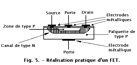
The exact design of the F.E.T. is given in figure 5.
The P-type wafer, on which the various operations were carried out, constitutes the zones P of the door. The latter, as well as the zone N located between the doors, are provided with metal electrodes for the connection of the component.
So far we have only considered F.E.T. consisting of an N-type channel located between two P-type zones.
For these, the current flowing between SOURCE and DRAIN consists of electrons. However, F.E.T. is also manufactured. P-channel, whose door consists of two N.
The current is then formed of HOLES. The operation does not differ from that of F.E.T. Of course, the F.E.T. P-channel, requires voltages of opposite polarities compared to those of the F.E.T. N channel
It is still possible to increase the value of the input resistance by making transistors whose structure and operation differ from the F.E.T. at junctions.
This new type of transistor designated by the abbreviation MOS F.E.T.has the particularity of having the DOOR ISOLATED with respect to the channel.
The abbreviation MOS F.E.T. comes from the Anglo-Saxon terms "Metal Oxide Semi-conductor, Fild Effect Transistor" meaning Field Effect Transistor, Metal Oxide Semiconductor.
The last three words indicate the particular structure of this transistor that we will describe.
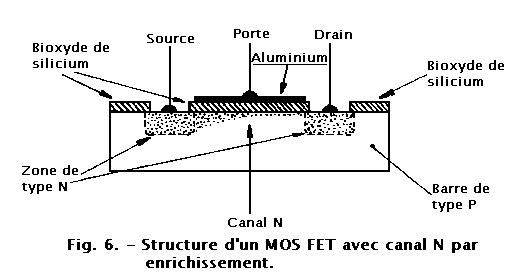
The MOS F.E.T. (shown in Figure 6) is produced on a P-type silicon wafer, on one side of which high-doping N-type zones are formed by diffusion.
On this same side, a very thin insulating layer of SILICON BIOXIDE, obtained by evaporation, is deposited. This insulating layer does not cover the entire surface, because at the time of the deposition of the dioxide, the two N zones are left open, so that the metal electrodes, one of which is SOURCE and the other DRAIN, can be placed there. Finally, on the surface of the silicon dioxide layer between the two P zones, an aluminum layer is added, constituting the DOOR.
This is obviously isolated from the semiconductor substance, by means of the interposed layer of dioxide.
The three words "metal, oxide, semiconductor" of which we spoke, indicate precisely the succession of the various elements corresponding to the DOOR. Indeed, referring to Figure 6, we meet from top to bottom :
aluminum (metal)
the oxide (oxide)
silicon (semiconductor)
The operation of the MOS F.E.T. is the next :
By applying a voltage between the DOOR and the SOURCE, so as to make the first positive with respect to the second, the DOOR is positive with respect to the silicon wafer P.
As a result, the positive moving charges of silicon P are pushed towards the inside of the wafer, while the negative mobile charges of the source are attracted to the surface.
More precisely, on the surface of the wafer relative to the layer of silicon dioxide located under the door, a layer of negative mobile charges is formed, establishing a connection between the SOURCE and the DRAIN and forming an N-channel, as shown Figure 6.
This channel has a certain resistance, which can be reduced by increasing the voltage applied to the door. Under the effect of voltage, the number of electrons present in the channel increases.
On the other hand, by applying an adequate voltage between the DRAIN and the SOURCE, one obtains an absorption current, due to the electrons of the channel connecting the two electrodes.
The intensity of this current can be varied by changing the value of the voltage applied between the DOOR and the SOURCE. Although the DOOR is now positive with respect to SOURCE, there is no current flowing through it because the silicon dioxide layer completely isolates it from the channel. Therefore, the ENTRY RESISTANCE OF MOS F.E.T. reaches values of the order of BILLION DE MEGOHMS.
In fact, the gate and the wafer of the MOS F.E.T. semiconductor, being reciprocally isolated by means of the silicon dioxide layer, behave as the two plates of a capacitor.
The control voltage creates an electric field between these two electrodes, field having an influence on the number of electrons present in the channel. Thus, it is possible to control the absorption current.
The transistors of the type which we have just studied are called "field effect" precisely by the fact that the control of the absorption current is carried out using the effect produced by an electric field.
In ordinary transistors, on the other hand, the control of the collector current is obtained by means of another current.
F.E.T. MOS can operate in two different ways : either by ENRICHMENT or by RAREFACTION, depending on the type of construction adopted.
When the MOS F.E.T. consists of an N channel, located between two heavily doped N-type zones, while the DOOR extends along the entire channel (Figure 6), the operation is by ENRICHMENT. Indeed, by making the DOOR positive with respect to the SOURCE, one enriches the channel of electrons, thus reducing the resistance between the SOURCE and the DRAIN.
In this case, if the voltage applied to the gate is zero, the number of electrons in the channel is very small and the absorption current virtually zero.
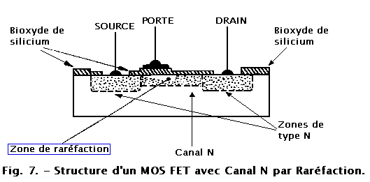
The MOS F.E.T. The enrichment process has a drawback : a very important capacitance between the gate and the wafer of the semiconductor. This ability can be reduced by using a door that covers only a portion of the channel (Figure 7).
However, this solution has the disadvantage of causing a very high resistance in the part of the channel not being enriched with electrons.
This disadvantage is remedied by adequate doping, making it possible to obtain a low-resistance channel, even when the voltage applied to the door is zero.
We thus arrive at a MOS F.E.T., whose CANAL, SOURCE and DRAIN are constituted by the same N-type material (the SOURCE and the DRAIN however being more strongly doped) and whose operation is carried out by RAREFACTION. In this case, by applying a negative voltage to the DOOR, it pushes back the electrons of the channel, producing a zone of rarefaction of the charges (Figure 7).
Therefore, the absorption current vanishes only when the negative voltage applied to the gate reaches a value sufficient to determine the "blocking" of the channel.
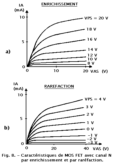
The characteristics of the absorption current of a F.E.T. enrichment type, differ from those of a MOS F.E.T. rarefaction, especially with regard to the values of the voltage applied between the DOOR and the SOURCE.
Figure 8 highlights the difference that characterizes these two types.
In the case of the enrichment type (Figure 8-a), the VPS voltages have exclusively positive values, between 8 and 20 volts.
For the rarefaction type (Figure 8-b), these same voltages are negative or positive and between -3 V and +4 V.
Note that the MOS F.E.T. can be made with a P-channel. In this case, previous observations about F.E.T. at junction remain valid.
The UNI-JUNCTION transistor owes its name to the fact that it has only one junction. This type of transistor is often identified by the acronym U.J.T. of the English "Uni-Junction Transistor".
This property allows particular uses, among which one can quote the generators of pulses, necessary to the control of thyristors (switching transistors of which we will study the characteristics in the next lesson "Semiconductors 8").
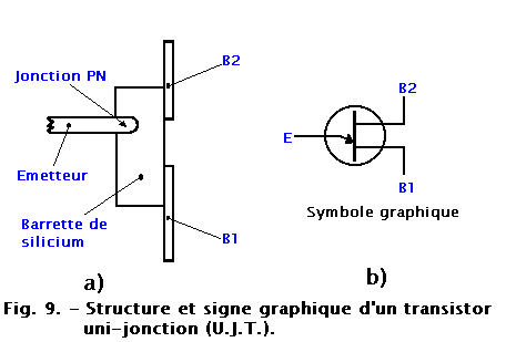
To understand the operation of a UNI-JUNCTION transistor, it is necessary to examine its structure by referring to Figure 9-a. Figure 9-b shows the schematic symbol adopted for the representation of the U.J.T.
This component consists mainly of an N SILICON BARRETTE, at the ends of which are arranged two contacts, called "first base (B1) and second base (B2)". These contacts are of the purely ohmic type, that is to say between them and the silicon bar, there is NO JUNCTION.
The only P.N. junction is between the bar and the E electrode, corresponding to the transmitter. This electrode is placed closer to the second base than the first, as can be seen in Figure 9-a.
The silicon N bar has the normal characteristics of a resistor and its value is between 5 W and 10 kW.
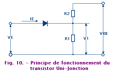
A voltage VBB is applied between the two bases, so as to make the second positive with respect to the first. Under the effect of this voltage, the N SILICON BARRETTE is traversed by a current, consisting of electrons, moving from the first base to the second.
Under the effect of this resistance presented by the bar, the current produces a voltage drop in it.
To see how the distribution of the voltage is performed along the strip, the transistor is shown as shown in Figure 10.
By means of the resistors R1 and R2, the silicon resistance is inserted between the first base and the emitter and between the latter and the SECOND BASE.
In Figure 10, V1 indicates the voltage drop across R1 (voltage present on the cathode of the diode).
By applying on the anode, a voltage VE less than V1, the diode is polarized in the opposite direction and the current can not circulate. On the other hand, if VE has a value greater than V1, the diode is forward biased ; in this case, an emitter current IE flows in the direction indicated in Figure 10.
THIS CURRENT IS ESSENTIALLY CONSISTING OF HOLES DIRECTING FROM THE BAR TO THE FIRST BASE.
These holes are the equivalent of the electrons present in the zone between the emitter and the first base, zone where an increase in the number of carriers occurs. This means that the resistance of this zone is reduced and consequently it can be traversed by a higher current, coming from the transmitter.
However, a more intense emitter current introduces a greater number of carriers and causes a further decrease in the resistance. This results in an even more intense current, so a further decrease in resistance and so on.
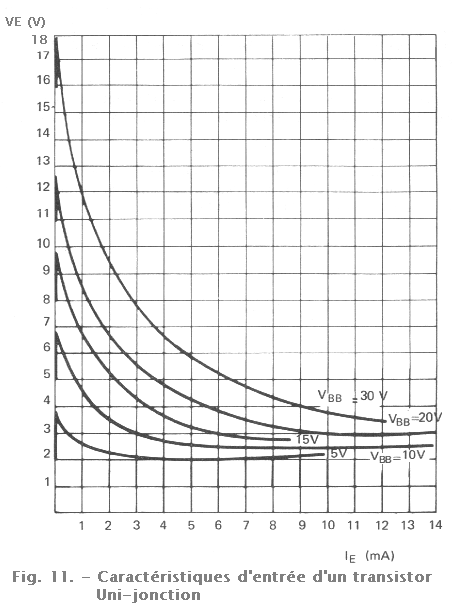
It may be thought that the current increases to extremely high values ; however, it is not so because at the same time as the current increases, the emitter voltage decreases. This fact is easily controllable by raising the characteristics, indicating how the emitter voltage VE varies, as a function of the current IE.
These characteristics are shown in Figure 11. Each of them refers to a particular value of the voltage VBB.
Consider for example the curve relating to VBB = 15 V.
For a zero value of the current IE, the curve has a vertical line, corresponding to the moment when the junction between the emitter and the silicon strip is inversely polarized.
When the voltage VE reaches a value of about 10 V, this same junction is polarized in the forward direction and therefore, the emitter current begins to flow. As this current increases in intensity, the voltage VE decreases and approaches the horizontal axis.
When an element behaves this way, it is said to have a negative resistance.
This property is very useful for the realization of many circuits, capable of generating particular waveforms. Indeed, this type of transistor behaves like a switch which, depending on the value of the voltage applied to the transmitter, is OPEN (high input impedance) or CLOSE (low input impedance).
We therefore find that the UNI-JUNCTION transistor has applications different from those of the transistors studied previously.
We end here the technology of the transistors. In the next lessons, we will study the THYRISTOR, DIAC and TRIAC and finally we will start the lessons of digital electronics.


 Field Effect Transistors
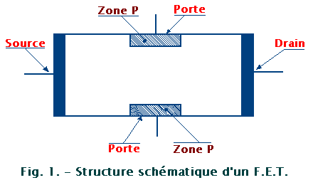
 Click here for the next lesson or in the summary provided for this purpose.
 Top of page
 Next Page