Thyristors - The Triacs - The Diacs - The Shockley Diode :
In this lesson we will study three new types of semiconductors, especially used in the field of switching. These are THYRISTOR, DIAC and TRIAC. Especially used in the field of switching. THYRISTOR, DIAC and TRIAC.
What is the THYRISTOR ?
It is an almost perfect switch, both unidirectional rectifier and amplifier.
As for the DIAC, it is a bidirectional device, becoming conductive when the applied voltage exceeds a certain threshold.
Finally the TRIAC, of the same family as the thyristor, differs from the latter by the fact that it is bidirectional.
After having seen these three new elements, we will finish this last lesson of BASIC ELECTRONICS BASE course, by the examination of the new lessons of digital electronics but before, we will also finish some fundamental assemblies such as the triode and the multivibrators to electronic and transistor-based tuiles that will be seen after this lesson.
The thyristor is a particular silicon diode, having a CONTROL CIRCUIT. This element can go from the PROHIBITION state to the CONDUCTION state but as soon as it is reached, the control electrode can no longer control the current flow.
The structure of this component is quite complex. Indeed, a THYRISTOR comprises THREE JUNCTIONS, consisting of two N zones and two P zones (Figure 1).
The lowest P zone is the ANODE of the diode, while the CATHODE is formed by the highest N zone.
The zone P under the cathode is the Trigger and therefore has the necessary contact for the connection to the external circuit.
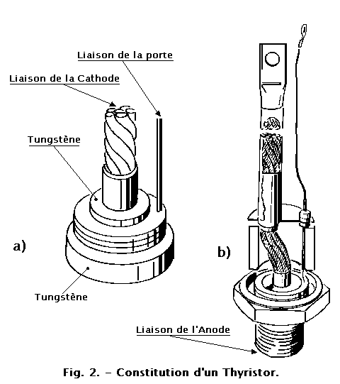
All these different areas, formed by the methods described in the previous lessons, is reinforced by two tungsten disks, as can be seen in Figure 2.
One of these disks carries a braided connection cable, corresponding to the CATHODE. This set is enclosed in a hermetic case, whose base ends with a thread corresponding to the ANODE.
It also allows to fix a metal plate, serving as a radiator, to dissipate heat that may damage the component.
Let's see how the THYRISTOR works.
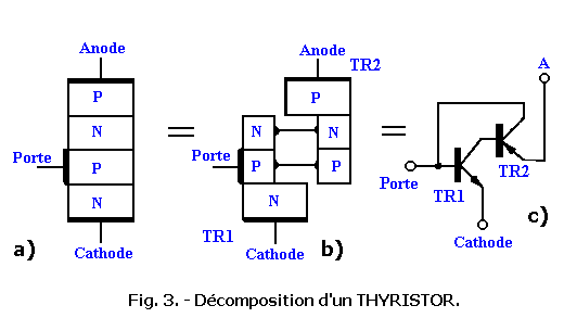
Consider for this purpose Figure 3-a, representing the thyristor of Figure 1, in another form.
Suppose that we cut the two central blocks, so as to break the thyristor into two parts. Connect these together, by means of connection, as in Figure 3-b.
One of the two parts thus obtained is formed of a block P, located between two N blocks, constituting a N.P.N. type transistor. (TR1 in Figure 3-b).
The other part is formed of a silicon block N, located between two blocks P, constituting a transistor of the P.N.P. (TR2 in Figure 3-b)
Representing these two transistors and connecting them as in Figure 3-b, we obtain the representation of Figure 3-c.
Each transistor has its base connected directly to the collector of the other and the assembly comprises three output links (A, C and P), corresponding to the anode, the cathode and the trigger (also called the DOOR).
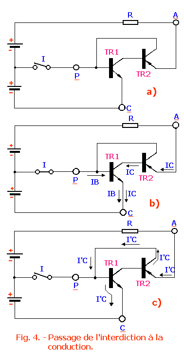
Feed the circuit using two batteries, mounted as in Figure 4-a.
Under these conditions, the transmitter of TR2 (corresponding to the ANODE of the thyristor) is positive with respect to the transmitter of TR1 (corresponding to the CATHODE of this thyristor). Although this component has its positive anode relative to its cathode, no current can flow when the switch (I) is open. Indeed, since the base current of TR1 is zero, the collector current is also zero.
Since the base of TR1 is connected directly to the base of TR2, which is true for the first transistor is also valid for the second.
By closing switch I, the base-emitter junction of TR1 is forward biased, since the base is positive with respect to the transmitter. Therefore, this junction is crossed by a direct current IB, in the direction indicated by the arrows (Figure 4-b). This current determines the passage of a collector current IC in TR1, and also passes through the emitter-base junction of TR2.
Since the current IC passes through the emitter-base junction of TR2, it determines the passage of a new current I'C in the latter transistor. This current flows through the circuit in the direction indicated by the arrows (Figure 4-c), that is to say, it crosses the base-emitter junction of TR1, in the same direction as the current IB (Figure 4-b).
The current flowing through the base-emitter junction of TR1 has therefore increased, the current I'C being added to IB. As a result, the current IC of TR1 also increases, and, crossing the emitter-base junction of TR2, in turn produces an increase in IC.
The current passing through the base-emitter junction of TR1 is therefore as well as the current IC and the current I'C, and so on.
It is thus understood how, by the action of each transistor on one another, the current which passes between the point A and the point C, that is to say between the anode and the cathode increases until to a limit value determined solely by the resistor R, which is in series in the circuit.
When this limit value is reached, switch I can be opened, as shown in Figure 4-c. The transistors are in fact now able to maintain one and the other in the conduction state.
It can thus be seen that the THYRISTOR CAN PASS FROM THE PROHIBITED STATE TO THE CONDUCTION STATE, by briefly applying an appropriate current to the TRIGGER circuit.
The fact that the current continues to flow after opening the switch I means that the TRIGGER can no longer affect the value of it. To reset the thyristor as soon as possible, simply apply a negative voltage to the anode.
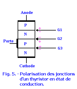
To understand what happens in this case, we must refer to the structure of the thyristor and examine the polarization, when the latter is in a state of conduction (Figure 5).
In this case, the three junctions are polarized in the forward direction and close to each of them, there is a large number of holes or free electrons.
By applying the negative voltage to the anode, the current flowing through the diode is interrupted and the flow of a reverse current is observed, due to the fact that the free charges are remote from the junctions marked by G1 and G3 in Figure 5.
After displacement of these charges, the reverse current ceases and the junctions G1 and G3 are polarized in opposite direction. The thyristor is however not in a condition of prohibition, because there is still a considerable number of holes and free electrons, near G2. These latter free charges are reciprocally eliminated by recombination insofar as the junctions G1 and G3 are polarized in the opposite direction.
When this recombination is complete, a positive voltage can be applied to the anode, without returning the thyristor to the conduction state. At this time, the trigger has taken over the possibility of controlling the thyristor.
The time that elapses between the moment when the flow of current stops and the moment when a positive voltage can be re-applied to the anode, without the thyristor returning to conduction, is called RETURN TIME. STATE OF PROHIBITION ; it is normally between 10 µ seconds and 15 µ seconds.
ItIt should be noted that in Figure 4-a, to simplify the explanation, it was assumed that when the THYRISTOR is prohibited, it is not crossed by a current, but this is not strictly accurate.
In fact, each of the two transistors composing the THYRISTOR is traversed by a residual current, as seen in the previous lessons concerning the transistors. This current flows, even when the basic circuit is open.
Thus, the residual current of the two transistors representing the thyristor circulates in the direction indicated in Figure 4 for the collector currents, but given its small intensity, it is not sufficient to bring the diode, under normal operating conditions, to the conduction state.
However, the presence of this residual current causes the diode to go from prohibition to conduction, even if the trigger current is zero.
This can be verified by applying a DC voltage of appropriate value to the anode of the thyristor. This voltage gives the carriers constituting the residual current, sufficient energy to release other carriers in greater numbers, these, in turn releasing other charges and so on.
The AVALANCHE EFFECT then occurs. As a result, the current increases very rapidly and the thyristor thus goes from the forbidden state to the conduction state.
It is good to insist on this phenomenon, having a certain influence, during the survey of the characteristics.
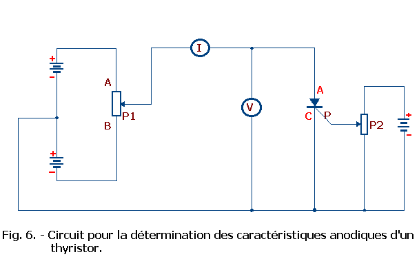
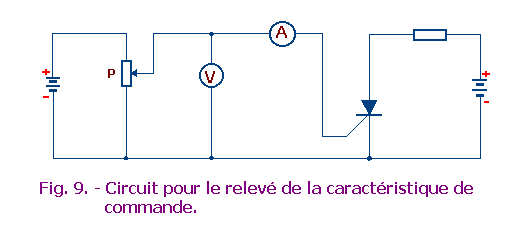
To determine these, to know how the anode current (Ia) varies as a function of the anode voltage (Va), for different values of the gate current (Ip), the circuit shown in Figure 6 is used.
In this figure, we can see the graphical symbol of the thyristor, similar to that of a diode, with in addition, on the cathode side, an electrode corresponding to the DOOR.
By means of P1, it is possible to vary the anode voltage (Va), indicated by the measuring instrument V, while the apparatus (I) indicates the values of the current, corresponding to the different voltages.
As for P2, it serves to adjust the voltage applied between the door and the cathode, that is to say, in practice, to dose the current of the gate circuit.
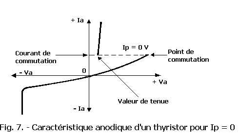
When this current has a value of zero, by varying the anode voltage, it is possible to determine the characteristic relating to Ip = 0 V.
The appearance of the latter is shown in Figure 7. It can be seen that when the anode voltage goes from a zero value to a positive voltage (+ Va), the anode current, constituted by the residual current, first increases progressively. because of the AVALANCHE EFFECT.
This current thus reaches the SWITCH POINT, corresponding to a sufficient value, to bring the thyristor from the forbidden state to the conduction state.
This is called SWITCHING CURRENT.
As soon as the thyristor is switched to the conduction state, the anode voltage must be reduced to prevent the anode current from taking excessive values.
We can see that the characteristic is almost vertical.
It can be deduced that low anodic voltages are sufficient to obtain high anode currents.
The thyristor remains in the conduction state, even if the anode voltage falls to fairly low values, provided that it does not fall below a value, called HOLD VALUE.
Below this, the thyristor returns to the forbidden state. On the other hand, when the anode voltage increases towards negative values (-Va), the characteristic takes a shape very similar to that of a normal diode, polarized in opposite direction (Figure 7).
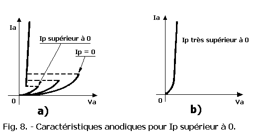
In Figure 8-a, on the contrary, the modification of the anode characteristic can be seen when the TRIGGER current takes values greater than zero.
It can be noted the decrease of the anode voltage, according to which is the switching current.
If the trigger current is much greater than zero, the characteristic takes the form shown in Figure 8-b. This pace is very similar to that of the characteristic of a P.N. junction.
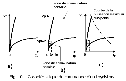
For the use of a THYRISTOR, it is also necessary to know the control characteristic, ie the characteristic showing how the trigger current Ip varies, when the voltage Vp, applied between the trigger and the cathode, is modified.
The values of these quantities can be found by means of the circuit of Figure 9.
By plotting on a diagram the values of the voltage and the current thus determined, it is possible to trace the control characteristic of the thyristor considered.
By redoing this plot with another thyristor of the same type, we would find a characteristic that could be very different. This fact is due to the inevitable construction differences that we encounter in these components.
For this reason, the control characteristics of the thyristors, provided by the manufacturers, comprise two curves, delimiting an area in which the characteristic can be, for a given type of thyristor.
It should be remembered that by increasing the voltage of the gate Vp, one reaches a value, in correspondence of which the trigger current Ip, is sufficient to cause conduction of the thyristor.
Because of construction differences, these values vary from one thyristor to another for the same type of component.
The shaded area of Figure 10-b indicates the possible switching points. It is delimited by the values Vpmin and Ipmin.
This surface therefore represents the zone in which switching is possible, but not certain, while the upper zone indicates the values where switching is certain in all cases.
It should be noted that not all values in the upper zone can be adopted for the control of a thyristor. Indeed, for some of these values the power dissipated in the junction gate-cathode, would exceed the possibilities of the thyristor. As a result, the maximum power dissipable safely, is indicated by the dashed curve.
The control characteristic, in its final appearance, is shown in Figure 10-c.
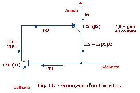
The triggering of the thyristor by its trigger or gate, is the most common priming system.
The thyristor is mounted on the circuit, so as to be forward biased (see Figure 11).
A POSITIVE IMPULSION is applied to the trigger (IG).
The transistor TR1 thus receives IG as base current. As a result, its collector current passes IG1,
(où 1
= current gain of TR1). This current is in turn injected into the base of TR2, which then delivers a current IG1 2
(where 2
= current gain of TR2).
This same current IG 1 2
TR2 collector current is reinjected on the basis of TR1.
Two cases must then be considered.
1°) The product 1 2
is smaller than 1 : THE DEVICE DOES NOT INITIATE.
2°) The product1 2
is close to unity : the process of the amplification is manifested and the thyristor goes to the conductive state.
These two conditions (1 2
< 1 and1
2
close to 1) characterize the state of the thyristor as a function of the current.
The gain
of a silicon transistor generally increases with the current (more exactly the gain in current increases with the emitter current).
With a low gate current, the product 12
is less than 1. The thyristor remains blocked.
With a higher value trigger current, that is, with a sufficient control pulse, the emitter currents are high enough for 1 2
gives a value tending towards unity, that is 12
-------> 1.
As soon as the priming is performed, the positive reaction (the collector current of each transistor being applied to the bases of the other transistor) causes TR1 and TR2 to saturation. These two components remain in this state even if the control signal disappears.
As we have just said, the essential property of a silicon transistor is to have a current gain, increasing with the emitter current IE. Because of this, all the causes likely to cause an increase in the current IE make it possible to trigger the priming.
We can therefore act :
1°)ON THE VOLTAGE : If the cathode-anode voltage increases, there comes a time when the LEAKAGE CURRENT is sufficient to trigger a rapid increase of IE, thus to cause the priming.
2°) THE SLOPE OF THE VOLTAGE : The PN junction has a certain CAPACITY. Thus, by suddenly increasing the anode-cathode voltage, this capacity is charged and a current of :
i = (C V)
/ t
C = capacity value of the junction
V (delta V) = variation of the voltage
t (delta t) =duration of variation
When the current (i) reaches a certain value, priming occurs.
3°) TEMPERATURE : The reverse leakage current of a silicon transistor doubles approximately every 14° C (when the temperature rises).
Again, when the leakage current is sufficient, the thyristor starts.
We only mentioned these possibilities for information purposes, because in the great majority of cases, THYRISTOR TRIGGERING is triggered by injecting a command PULSE on the TRIGGER, that is to say using the TRANSISTOR EFFECT.
1. 3. -
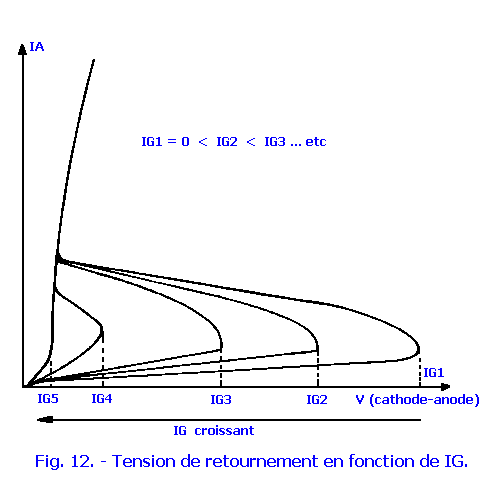
VOLTAGE OF REVERSAL
As we just said in the previous paragraph, it is possible to start a thyristor, by acting on the THODE-ANODE VOLTAGE.
The value of the voltage for which the thyristor starts is called the inverting voltage. The value of this voltage, however, depends on the control signal, possibly applied to the trigger. Figure 12 highlights this relationship.
When the trigger current IG is zero (in Figure 12, IG1 = 0), the anode-cathode voltage must reach the reversal voltage for the thyristor to start. On the other hand with an increasing gate current, the reversal voltage drops to much lower values.
At the limit, the thyristor behaves like a diode (for IG5, in Figure 12). This means that if the trigger current is strong enough, a small anode voltage is sufficient to trigger.
Also, to prevent erratic priming, you can mount a resistance between the trigger and the cathode.
Very often manufacturers also integrate by diffusion, this resistance in the thyristor (SHORTED EMITTER technique).
It has the effect of requiring a more intense trigger current, for the priming of the thyristor, but by the same, improves its holding in the off state.
Thyristors are increasingly used in current control circuits.
Research in this area has enabled the production of thyristors capable of passing an intensity of the order of several hundred amperes, with a reverse peak voltage of 1200 volts.
Such thyristors are, however, reserved for very special purposes. In the current domain, we find especially :
THYRISTORS at low current < 1 A
THYRISTORS with high current 1 to 35 A
THYRISTORS high power 35 to 150 A (approximately).
The applications of thyristors are very large and more particularly in industrial electronics.
They are also found in some household appliances, where they can in addition to a specific function, replace a transformer.
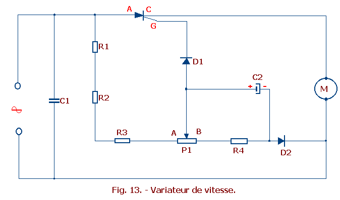
Figure 13 illustrates a common application : THE SPEED DRIVE.
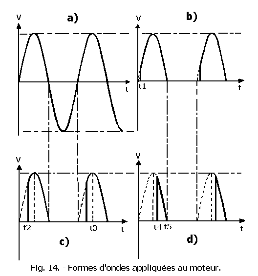
Taken directly on the sector, the tension has the sinusoidal pace, represented Figure 14-a.
By inserting the circuit of Figure 13, the maximum voltage is only half a sinusoid. In this case, the thyristor behaves like a diode (Figure 14-b).
Thus, by inserting the device between the mains plug and the motor, the speed of the motor M decreases ; we use only the positive alternations to feed it.
To further reduce the speed, it acts on the potentiometer P1. The voltage that then powers the motor takes the shape shown in Figure 14-c. We note that only a part of the positive half-cycle remains.
By continuing to act on P1, we can manage to have only a small part of the positive half-cycle (Figure 14-d) or even nothing at all, that is to say, complete suppression of positive alternation.
One essential fact must be noted : The DECREASE OF SPEED is carried out without REDUCING THE VOLTAGE APPLIED TO THE ENGINE (except at very low speed) but only by ACTING on the CONDUCTION TIME. This means that the engine retains almost all of its power, whatever its speed.
In a circuit of this type, the trigger control voltage is obtained by a divider bridge R1, R2 and R3, connected between the anode of the thyristor and the potentiometer P1.
When the voltage applied to the anode of the thyristor increases positively, that applied to the trigger also increases, since it is transmitted by D1. In this way, one thus reaches the value necessary to trigger the conduction of the thyristor. This value is reached in different times, depending on the position of the fader.
When the cursor is at A, the triggering voltage is reached shortly after the beginning of the positive half cycle (as shown in Figure 14-b
By moving the cursor from P1 to B, the control voltage is reduced by the introduction of additional resistance ; the conduction of the thyristor occurs only a certain time after the beginning of the positive half cycle (case illustrated in Figure 14-c).
From what has been said, one might think that it is impossible to leave the THYRISTOR conductive after time t3 (Figure 14), but we see that this is possible (Figure 14-d).
This result is achieved by the capacitor C2, which determines a phase shift between the voltage of the sector present on the anode of the thyristor and the gate voltage.
The two tensions do not vary together, the second is DELAY on the first. Indeed, the gate voltage reaches its maximum positive, while the anode voltage of the thyristor has already begun to decrease.
The conduction time between t4 and t5 is obviously very short, which means that the speed of the motor is then very low.
At the end of any positive alternation, the mains voltage is canceled, INTERRUPTING the conduction of the thyristor.
During the negative half-waves, the diodes D1 and D2 are polarized in the opposite direction and the system remains blocked.
Conduction resumes at the next positive half-cycle, first in the diodes, then in the thyristor, when the trigger voltage is reached.
When the power supply voltage of the motor looks like Figure 14-d (almost impulse), there is noise in the radio frequencies, which can disturb the radio reception. To eliminate this disadvantage, a capacitor C1 has been placed to reduce these disorders to a large extent.
This assembly is given here as an example of application of thyristors, found in many circuits in INDUSTRIAL ELECTRONICS.
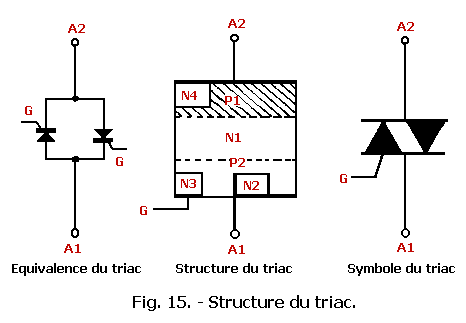
The TRIAC is a semiconductor device with three electrodes (anode 1, anode 2, trigger) that can go from the off state to the conduction state in its two directions of polarization. In other words, it is a component of the same family as the thyristor, but which is BIDIRECTIONAL (the thyristor being unidirectional).
The TRIAC can also be compared to two thyristors in parallel, mounted upside down (Figure 15).
TRIAC can be considered as a STRUCTURE P1 N1 P2 N2 of thyristor, in which A1 is the cathode (connected to N2), A2 the anode (connected to P1) G, the trigger (connected to P2), but with in more :
A1 also related to P2
B2 also connected to an additional layer N4
G also connected to an additional layer N3
The structure P2 N1 P1 N4, thus constitutes a second thyristor, connected in inverse parallel with the thyristor P1 N1 P2 N2.
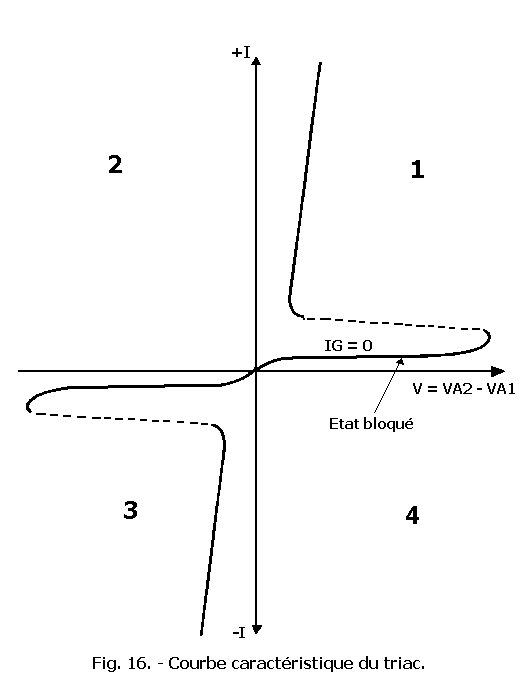
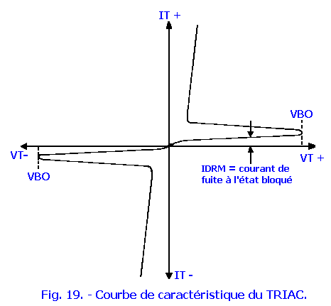
The voltage-current characteristic is symmetrical (figure 16 below).
This device can switch from a blocked state to a conductive state in both directions of polarization (quadrant 1 and 3) and return to the off state by inverting voltage or decreasing the current below the value of the holding current IH.
In the absence of a signal on the trigger, the device can be considered as two polarized rectifiers in the opposite direction. No current flows in the triac, therefore in the load (except a very slight leakage current).
It is therefore admitted that the TRIAC behaves like an open switch. However, according to the polarization one can have the following states :
1°) If A2 is at a positive potential of 1.5 volts with respect to A1, a positive or negative tension of suitable value, applied on the trigger, causes the priming : THE TRIAC begins to lead.
2°) If A2 is at a negative potential of 1.5 volts with respect to A1, a positive or negative voltage of suitable value, applied on the trigger, causes the priming : THE TRIAC begins to drive.
3°) If the current going from A2 to A1 or from A1 to A2 is established, the TRIAC is LOCKED and the trigger voltage can be suppressed, it is POSITIVE or NEGATIVE : THE TRIAC remains in state of conduction.
4°) When the current in the TRIAC is established (in one direction or in the other), it is necessary to block it, to reduce the intensity of this current, to a value close to zero.
The minimum intensity for which the TRIAC remains conductive is called the minimum holding intensity (HI).
The above condition (current close to zero), obviously exists whenever the AC voltage of the network goes through zero, that is to say at each half-wave.
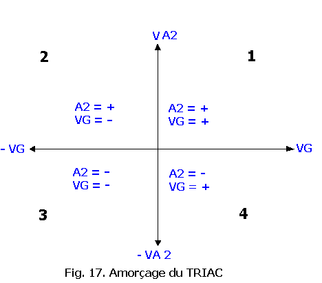
As we have just seen, the TRIAC can be triggered by a POSITIVE or NEGATIVE pulse on the TRIG, regardless of the polarity of A2 relative to A1. However, there is a PREFERENTIAL SENSE, illustrated Figure 17.
When tripping has occurred, the internal resistance of the triac is low ; as a result, the voltage drop between A2 and A1 is also low (about 1.2 volts). This means that the power dissipated in pure loss in the TRIAC is very small compared to the power of the load.
Let us also mention that a TRIAC can withstand, without inconvenience, brief, rather intense, overloads. Thus, a TRIAC of 6 amps for example can withstand during a few alternations, a current of the order of 100 amperes.
This feature is very interesting, because when starting a motor for example, the instantaneous intensity required, is much larger than the intensity of operation of the engine in normal mode.
By applying a voltage V1 to A1, V2 to A2 and VG to the TRIGGER, taking V1 as a reference, that is to say V1 = 0, the four polarization quadrants of Figure 17 can be defined.
How does the boot occur in the 4 possible cases ?
a)PRIMING QUADRANT 1 (+ +)
In this case we have V2 > V1.
A positive pulse is applied on the trigger between G and A1 (+ on G).
By calling T
the thyristor P1 N1 P2 N2 having A2 as anode and A1 as cathode (see figure 15) and T' the thyristor P2 N1 P1 N4 with A1 as anode and A2 as cathode, we have :
T is under direct voltage ; the trigger positive current causes the triggering of T as a normal transistor.
b) PRIMING QUADRANT 3 (- -)
In this case we have V2 < V1
A negative pulse is applied on the trigger between and A1 (- on G).
The trigger current IG enters A1, through the diode P2 N3 in the forward direction and thus causes the collapse of the potential barrier P1 N1. Indeed, the diode P2 N3 is traversed by HOLES from P2 to N3 and electrons from N3 to P2.
These electrons diffuse through P2 to the junction P2 N1, which directs them in N1 (action of the junction on the minority carriers that reach it) ; this results in a reduction of the potential barrier P2 N1 and consequently an increase in the current of the HOLES from P2 to N1
These holes are absorbed by the junction P1 N1 whose inverse current increases, with the effect of initiating T'.
c) PRIMING QUADRANT 2 ( + - )
In this case we have V2 < V1
A negative pulse is applied on the trigger between G and A1 (- on G).
The tripping current flows from P2 to N3 and initiates T', as before.
d)PRIMING QUADRANT 4 ( - + )
In this case we have V2 < V1
A positive pulse is applied on the trigger between G and A1 (+ on G).
The triggering process can be compared to that of the first quadrant, so T conductive.
In reality, the phenomenon is more complex, because for a detailed and hypothetical study, the conduction zone N3 P2 N1 P1 should be considered, from which it appears that in the fourth quadrant, the trigger sensitivity is smaller than in other cases.
The two most used priming methods are those described in a) and b), that is to say the first and third quadrants. Indeed, when A2 and G have the same polarity, the trigger current necessary to cause the boot is much lower than when these polarities are opposite.
The PREFERENTIAL SENS of priming, with reference to Figure 17 is therefore the one where we have :
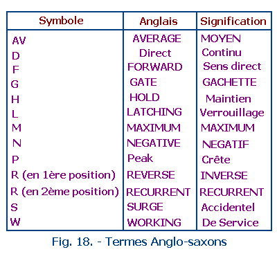
The most complete works dealing with thyristors and triacs being American (which explains the more and more frequent use of Anglo-Saxon terms in French texts and confirms that technical evolution has a certain influence on language), it is good to give the meaning of the symbols used to give the characteristics of these components (figure 18).
Extracted from a SILEC document (semiconductor manufacturer), here is how the essential characteristics of a TRIAC (type TTAL 220) are presented.
*** USE VALUES ***
ITeff
200 A
= Effective current in the on state.
ITRM
600 A = Peak current detected in the on state.
ITSM
1600 A à 50 Hz =
Maximum accidental peak current.
VDWM
200 V =
Maximum peak voltage in the off state.
VRSM
300 V =
Accidental spike reverse voltage.
*** TRIGGER CHARACTERISTICS ***
IFGM
5 A
= Peak direct current.
VFGM
10 V
= Peak direct voltage
VRGM
5 V =
Peak reverse voltage
PG
10 W
= Power trigger (English POWER GATE).
Other important features that should be mentioned include :
VBO= Maximum voltage that the component can withstand while remaining in the off state. If this voltage is exceeded the triac starts.
dv / dt= Maximum growth rate of the anode voltage that can be supported by the device, without risk of initiation.
di / dt= Maximum growth rate of the anode current that can be supported by the device without causing its destruction.
With the aid of these indications, the diagram of Figure 16 can thus be completed by the following indications (Figure 19).
The DIAC is a semiconductor component, used to TRIGGER thyristors and triacs.
It is a SYMMETRIC element, therefore a BIDIRECTIONAL component, becoming conductive when the voltage exceeds a certain threshold (overturning voltage).
Its structure is very simple, since it is a double diffusion of impurities TYPE OPPOSED to that of the substrate (monocrystal).
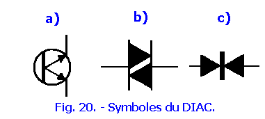
The symbol, or rather the symbols of the DIAC are represented in figure 20.
The symbol in Figure 20-b is questionable because it is virtually identical to that of TRIAC.
The symbol in Figure 20-c is the simplest and most easily understand the operation of this component.
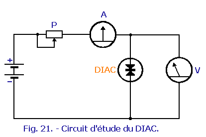
Let's see on this subject the behavior of the DIAC. For this purpose, let us refer to the diagram in Figure 21.
Let's set the potential P to its MAXIMUM VALUE. The voltage applied to the DIAC and read on the voltmeter V is very low ; the current measured by the ammeter A is also very low and corresponds to a very slight leakage current.
Maneuver P to increase the value of the voltage V.
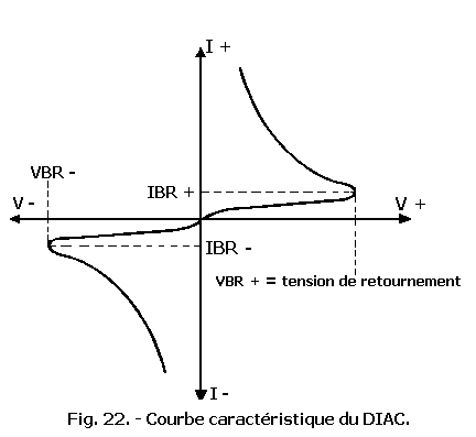
The current increases but very slightly, as can be seen in Figure 22 (IBR +), then suddenly, for a certain voltage value well determined, the current increases intensively and dynamic resistance DIAC BECOMES NEGATIVE. This means that this resistance while being of low value, increases according to the current.
Figure 22 illustrates what has just been said : (on the right side of the I axis).
If now, in a second experiment we reverse the battery of batteries, we see that the same phenomenon occurs, but in the opposite direction.
This produces a substantially symmetrical curve, as can be seen in Figure 22.
Based on the above, the following two conclusions can be drawn :
1°)
The DIAC is not a RECTIFIER.
2°) It is not possible to have between its terminals a voltage higher than VBR + and VBR -, without risk of destruction of the component.
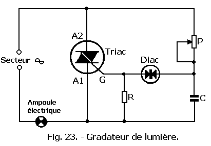
The DIAC is used in combination with the TRIAC, for the control of the latter.
One can for example make a LIGHT GRADER. In this type of mounting the THYRISTOR is not suitable, because since it only leads in one direction, a flicker of the bulb is noticeable, especially at low light intensities.
In this case, in fact, the conduction time with respect to complete alternation is very short. Thus, between each conduction period, the filament of the bulb cools down and results in a decrease in the emitted light.
When the thyristor drives again, the filament emits a stronger light again, followed by a decrease and so on.
The TRIAC being CONDUCTIVE in both directions of the AC voltage, avoids this flicker.
The typical assembly of a LIGHT GRADER is given in figure 23
Note that this same assembly can, without any modification, serve as SPEED DRIVE.
How does this circuit work ?
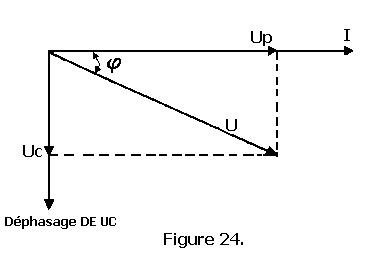
The right part of the diagram comprises a PHASING device consisting of a capacitor C and a potentiometer P.
Part of the power supplied by the sector passes through these two elements. This current generates across P, a voltage that is in phase with it.
This voltage is given by the law of ohm :
Up =RI
At the terminals of the capacitor, a voltage is also born, but it is DEPHASED, of p / 2 (90°) with respect to the current.
The value of this voltage is given by the formula :
Uc = 1 / (C x w) x I
The vector representation is that of Figure 24.
The vector U, a geometrical sum of Uc and of Up is out of phase with the current I. It is obvious that this phase shift (angle j) depends essentially on the two vectors Uc and Up, hence on C and P.
Now P is a potentiometer ; it is therefore sufficient to operate the cursor to modify the PHASE OF U with respect to I. But U is the voltage across the resistance-capacitance assembly, therefore the voltage of the sector. The PHRASE of Uc with respect to U, therefore also varies according to the setting of P.
In conclusion :
At the terminals of C there is a voltage whose phase varies with the value of P.
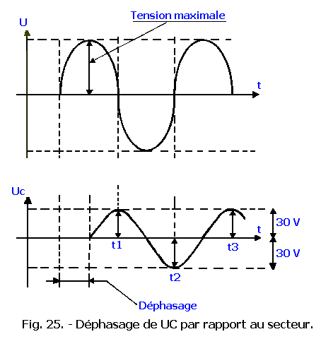
The Figure 25 represents the voltage U (immutable) of the voltage Uc, whose phase shift in time varies according to the value of R.
In general, the DIAC is triggered for a voltage close to 30 volts, which is to say that VBRof Figure 22 = 30 volts.
If P and C have been chosen judiciously, the maximum value of Uc can be equal to 30 Volts. This means that every time there is a voltage of 30 Volts across Uc, which occurs at times t1, t2, etc., there will be triggering DIAC, and therefore TRIAC.
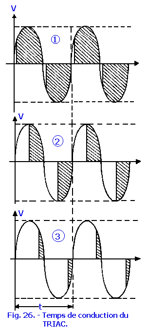
Figure 26 shows the shape of the voltage delivered by the TRIAC, that is, the CONDUCTION TIME of this element, as a function of three different settings of P.
1°) The electric bulb is fed almost normally. The conduction time of TRIAC is almost equal to t.
LONG CONDUCTION TIME (hatched portion).
2°) The light bulb is powered only half the time during each half-wave.
AVERAGE CONDUCTION TIME..
3°) The electric bulb is only fed during a fraction of time during each half-wave.
SHORT CONDUCTION TIME.
Note that in THYRISTORS DIMADERS or DIMMERS, one acts on the CONDUCTION TIME and not on the value of the voltage.
The DIAC is not the only component currently used for ordering TRIACS.
It must indeed be mentioned :
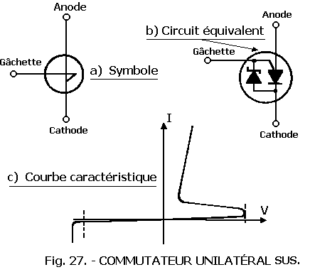
1°) THE UNILATERAL SWITCH (SUS).
This component, intended solely for triggering THYRISTORS consists of a miniature THYRISTOR and a ZENER diode.
Figure 27 shows the symbol of this component, its equivalent circuit and its characteristic curve.
We see that approximately, this set works as a DIAC which would be Unidirectional.
This switch has the advantage of triggering at FIXED VOLTAGE, determined by the ZENER DIODE.
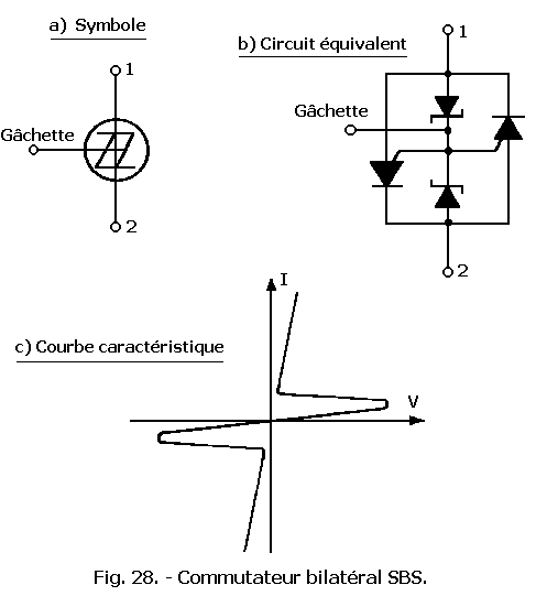
2°) THE BILATERAL SWITCH (SBS).
This component, derived from the previous SUS, is formed by two switches BILATERAL, mounted head to tail.
It works in both directions and is therefore mainly used for the control of TRIACS.
Figure 28 provides essential information on this element.
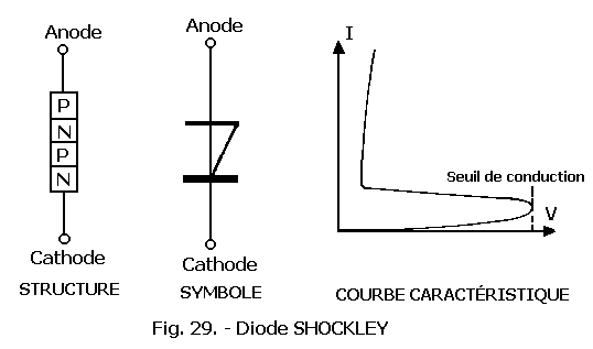
3°) THE SHOCKLEY DIODE
The SHOCKLEY diode, also called FOUR-LAYER DIODE or THYRISTOR DIODE is a UNIDIRECTIONAL BIPOLAR component.
of the PN PN type, this diode is comparable to a THYRISTOR which only includes ANODE and CATHODE.
Figure 29 shows the structure, symbol and characteristic curve of this component.
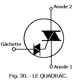
4°) THE QUADRAC.
The QUADRAC is not strictly speaking a tripping device, because it consists of a TRIAC, containing in the same housing a DIAC (Figure 30).
It is therefore only a compound element, the purpose of which is to simplify the circuits.
We thus finish our notions of fundamental electronics which, we hope, will help you to better understand the other parts of the new DIGITAL theoretical and practical lessons, will aim to explain the digital circuits concerning the computers including the integrated circuits for the least, to increase your knowledge in this field but, we will add other lessons about the fundamental montages to complete your general knowledge, in basic electronics, then we can detail the other parts of the lessons mentioned above.


 THE THYRISTOR
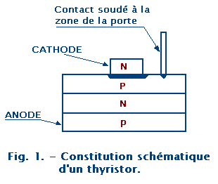
 Click here for the next lesson or in the summary provided for this purpose.
 Top of page
 Next Page