The semiconductors used for the manufacture of the devices of the same name are almost never of the intrinsic type. In intrinsic semiconductor is usually add a certain amount of foreign substances that spread throughout the crystal and alter the electrical state of the crystalline reticle. For this reason, we will examine the consequences of the presence of foreign atoms in the crystalline lattice of intrinsic semiconductors.
1. - SEMICONDUCTORS N AND P
Suppose that it is possible to intervene directly in the structure of a very pure and perfect tiny germanium crystal, within which there is a definite number of free electrons and an equal number of holes.
In this crystal and at any time, a portion of the free electrons returns to the valence band, as a result of energy losses due to shocks, but at the same time, other electrons move from the valence band to that of conduction. If the crystal temperature remains constant, the number of free electrons and holes also remain constant.
Now imagine that in the space of the crystalline reticle there are only two free electrons and two holes. By intervening in the structure of the crystal, three atoms of germanium are replaced by as many atoms of antimony (Figure 1).
This is of course an example whose sole purpose is to facilitate understanding. In practice, it never happens that a crystal placed at normal room temperature, has only two free electrons and two holes and even less a number of antimony atoms close to that of free electrons. In reality, the free electrons and holes contained in one cubic centimeter (cm3) of crystal are several thousand billion and the atoms of antimony are in a ratio of 1 in 1 000 000 germanium atoms.
The introduction of impurities (in this case antimony) into a semiconductor is called doping. This semiconductor is then doped.
Antimony is an element that belongs to group V of the MENDELEYEV classification (see previous semiconductor lesson). The outer layer of its atom has, indeed, five electrons. Four of these will help restore the covalent bonds with the nearby germanium atoms, while the fifth, finding no place in the covalent bonds, will remain bound to its own atom.
The link between the fifth peripheral electron of antimony and the corresponding atom, however, is not as strong as the covalent bonds. It will break easily and the fifth electron will enter the conduction band very quickly to reach the free electrons of the crystal.
Let us return to the example given previously which consisted of substituting three atoms of germanium with three atoms of antimony. By this operation, three new free electrons are introduced into the reticle of the crystal, which, added to the first two, bring the number of free electrons to five.
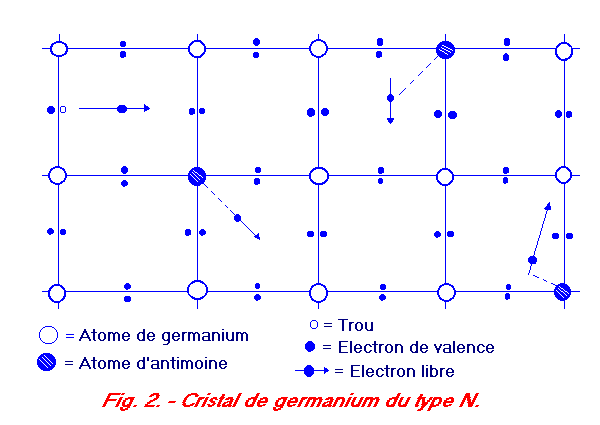
One might think that the reticle thus comprises five free electrons and two holes. In reality, some time after the substitution of germanium with antimony (and this when the temperature remains constant), there can be in the crystal only four free electrons and a single hole (Figure 2).
This phenomenon is explained by the fact that a certain number of free electrons occupy an equal number of holes, which inevitably leads to the disappearance of the latter.
Ultimately, the operation of substitution of germanium atoms by antimony atoms results in an increase in the number of free electrons which no longer corresponds, at a given moment, to the sum of the free electrons brought by the antimony and existing ones already. There is recombination of a portion of the free electrons and holes to form valence electrons.
Given what has just been said, we can already draw the following rule :
For any increase of the free electrons in a constant-temperature semiconductor crystal, there is a reduction in the number of holes, so that the product of the number of free electrons by the number of holes remains constant.
In the example of Figure 1, we saw at first two free electrons and two holes.
The product is 2 x 2 = 4
After the three atoms of germanium have been replaced by three atoms of antimony, the number of free electrons increases from 2 to 4, while the number of holes decreases from 2 to 1.
The product remains unchanged, that is to say 4 x 1 = 4.
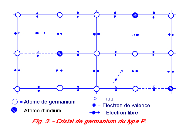
A similar situation is obtained by replacing the three germanium atoms with three indium atoms (Figure 3)..
Indium is an element that belongs to group III of the MENDELEYEV classification (see previous semiconductor lesson). The outer layer of its atom has indeed three electrons, that is to say one less than the four required to complete the covalent bonds with neighboring germanium atoms. After substituting three atoms of germanium with three indium atoms, we have inside the crystalline reticle three covalent bonds weakened by the absence of an electron, thus formation of the three new holes.
The weakened links are shown in Figures 3 and 4 by the dotted lines, ranging from indium atoms to one of the four surrounding germanium atoms.
The holes that appear with the weakened links are represented by small white circles, like those that formed in the covalent bonds, following the release of a valence electron.
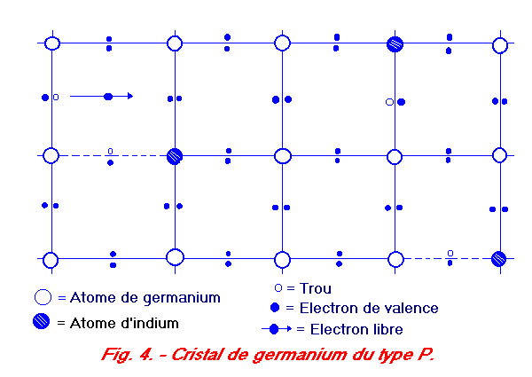
If we add the three holes introduced with the indium atoms to the two other holes existing in the intrinsic germanium, we should have five holes and two free electrons. In fact, and always at a constant temperature, it is possible, after substitution of germanium by indium, to have only four holes and a single free electron (Figure 4).
Here again, this phenomenon is explained by the fact that a part of the free electrons falls into the holes and remains there.
Ultimately, the operation of substitution of germanium atoms by indium atoms results in an increase in the number of holes which no longer corresponds, at a given moment, to the sum of the holes brought by indium and those existing already. Some of the holes and free electrons recombine to form the covalent bonds.
Here we can draw the following conclusion :
For any increase of holes in a semiconductor at constant temperature, there is a decrease of free electrons, so that the product of the number of holes by the free electrons remains constant.
In the example of Figures 3 and 4, as in that of Figures 1 and 2, the initial product of the holes by the free electrons is equal to 4.
After substitution of the three atoms of germanium by the three indium atoms, the number of holes increases from 2 to 4, while the number of free electrons decreases from 2 to 1.
The product remains unchanged : 4 x 1 = 4.
Given what has just been said, semiconductors can already be divided into three distinct categories.
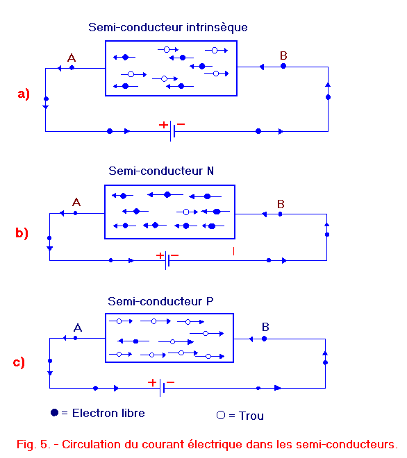
-Intrinsic semiconductors having a number of free electrons equal to that of the holes (Figure 5-a).
-The semiconductors N, obtained by introducing into a semiconductor crystal atoms of elements belonging to the group V of the table of MENDELEYEV. Here, the number of free electrons is much greater than that of holes (Figure 5-b).
- The semiconductors P, obtained by introducing into a semiconductor crystal atoms of elements belonging to group III of the table of MENDELEYEV. Here, the number of holes is much higher than that of free electrons (Figure 5-c).
The group V elements of the MENDELEYEV table used to form the N semiconductors are antimony, arsenic and phosphorus; they are called donors.
Group III elements used to form P semiconductors are indium, boron, gallium and aluminum ; they are called acceptors or receivers.
Let us now see how electrical conduction is performed in the three types of semiconductors listed above.
Figure 5-a shows a small block of intrinsic germanium traversed by the current produced by a battery. We notice inside the semiconductor, the birth of two flows of electrical charges.
The first consists of free electrons that go from the B end (negative side of the stack) to the A end (positive side of the stack). The second flow consists of holes which move from one atom to another inside the crystal reticle, go in the opposite direction to the previous, that is to say from the end A to the end B. Both flows consist of equal amounts of electrical charges, since in the intrinsic semiconductors the number of free electrons is equal to that of the holes.
The links placed between the end of the semiconductor and the battery are instead crossed by a single stream consisting solely of electrons.
Note that the current produced by a battery is continuous and its intensity is invariable in each section and at any point of the conductor. This means that at any moment, the same quantity of electrons enters the conductive wire through the A end and leaves the end B. The same quantity of electrons comes out and also enters through the ends of the small block (Figure 5-a).
To simplify all this, let's imagine that inside the semiconductor and at any moment, an electron leaves by the end A and another electron enters by the end B. We thus note that the number of electrons incoming is always equal to that of the outgoing electrons.
The outgoing electron belongs to the conduction band, that is to say it is a free electron. Thus, having no links with the crystalline reticle, it can freely leave the semiconductor and move towards the positive of the battery.
At the other end, the incoming electron encounters the holes that can move in the reticle and focus in the end connected to the negative of the stack, but can not leave the reticle. These holes are in fact essentially empty spaces in the valence band of the semiconductor atoms.
When the electron coming from the negative of the pile meets the holes, it occupies an empty place in the valence band, thus making a hole disappear.
Summarizing what has just been said, we can draw the following conclusion :
When one electron goes out and another goes in, there is always in the semiconductor the loss of a free electron and the disappearance of a hole.
If this process were repeated as many times as there are free electrons or holes, one might expect at a certain moment that the semiconductor remains without free electrons and without holes. In reality, the number of free electrons and holes present in the reticle depends exclusively on the temperature of the material. Indeed, if the temperature of the semiconductor block remains constant, for each missing electron-hole pair, it forms at one point of the semiconductor another free electron and another hole.
Thus, the two flows, that of the free electrons (which goes from the end B to the end A) and that of the holes (which in the same semiconductor circulates in the opposite direction) are fed in continuity, as long as the power generation by the battery.
In a semiconductor block N traversed by the current delivered by a battery (Figure 5-b), the phenomena of electrical conduction differ from those just described since the number of free electrons is greater than number of holes. In this case, two flows of electric charges are formed inside the semiconductor, one being stronger than the other. The free electrons that make up the upper flow are called majority carriers, while the holes that make up the lower flow are called minority carriers. There is indeed, in the semiconductor N, many more free electrons than holes.
It can therefore easily be understood that a large part of the electrons coming from the end B easily passes through the semiconductor block, always remaining in the conduction band.
In semiconductor P (Figure 5-c), two fluxes are also formed, but this time, the strongest flux consists of holes (majority carriers) and the weakest flow of free electrons (carriers minority). It is therefore unlikely that a free electron could cross the entire block from end B to that of A.
The free electrons coming out of the semiconductor and the holes that go from one end to the other of this same semiconductor generally originate near the A side. From this point, the two opposite charges are separate. The electron goes to the positive pole of the cell through the link and the hole goes to the B end of the block, where it will disappear as soon as its place is occupied by an electron coming from the negative of the cell.


 Footer
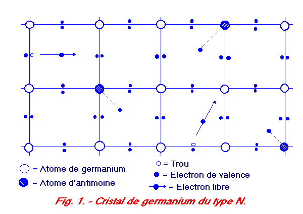
 Click here for the next lesson or in the summary provided for this purpose.
 Top of page
 Next Page