Structures of Crystals - Intrinsic Semiconductors :
2. - STRUCTURES OF CRYSTALS
The operation of the transistors depends on the properties of the outer layer of the atoms of certain bodies, called semiconductor bodies, but it is based on the state of aggregation of these bodies.
The fundamental physical characteristics of semiconductors occur exclusively when the material is in the solid state.
In addition, this material must be in a particular solid state called crystalline state. It is for this reason that transistors or semiconductor diodes are called crystal devices.
The crystalline state is distinguished from the other solid states by the fact that the atoms occupy in the aggregate a fixed position according to a repeated geometric design, more or less complex.
Take for example a very pure crystal of sodium chloride (cooking salt).
Sodium chloride is a compound consisting of chlorine and sodium atoms in equal parts. If we could enlarge a tiny grain of sodium chloride fifty million times, the atoms would appear as in figure 5-a.
This arrangement is repeated, always equal to itself, as the dimensions of the crystal grain increase.
The lattice structure of Figure 5-a is fundamental for many types of crystals. There are obviously other crystalline lattice structures of simple and compound substances.
Figure 5-b shows the representation of the selenium crystal, a simple substance used in the manufacture of solid rectifiers.
The atoms, in the crystalline structure of selenium, are arranged in spirals around parallel axes and these are grouped in superimposed layers.
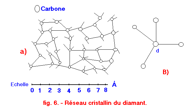
Among crystalline structures, that of diamond is of great importance in the study of semiconductors.
The diamond (Figure 6-a) is composed of carbon atoms, arranged so that each atom is surrounded by four others, all equidistant from the central atom and uniformly in the surrounding space (Figure 6- b).
The distance d between the central atom and the four neighboring atoms is constant in all points of the network (this distance is about 2 angstroms).
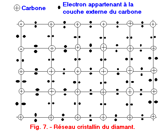
The crystal atoms are held together by covalent bonds, of the same type as those of Figure 4-b.
Recalling what has just been said about the nature of this connection, we can understand that the entire space between the atoms is occupied by an intense electronic circulation. Electrons walk in the empty spaces of the crystal lattice, passing from one orbit to another, but they are never really free : they always remain connected to the network formed by the atoms to which they initially belong. They could not, under the action of an external electric field, form a continual flow of current. In other words, it means that the diamond is a bad conductor of electricity.
To represent in a simpler way the crystalline structure of the diamond, one can resort to the plane representation (figure 7).
This figure shows more clearly that the distances between atoms are equal and makes it possible to better understand the existence of covalent bonds.
Semiconductors are substances whose electrical conductivity is intermediate between conductors and insulators.
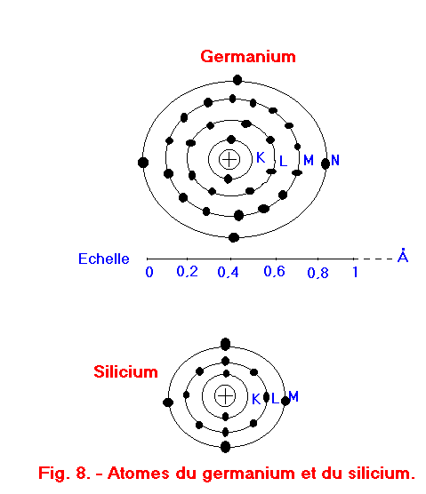
Copper oxide and selenium, used in some types of rectifiers, are semiconductors, as are various other oxides and metal salts, but germanium and silicon are the most important. Figure 8 shows the atom of each of these two elements.
It can be noted that for these two bodies, the outer layer of the atoms comprises only four electrons.
These elements are therefore of the tetravalent type, such as pure carbon (diamond).
Note also that carbon, silicon and germanium belong to the same group in the MENDELEYEV classification (group IV, figure 3). Thus, everything that has been said about the carbon lattice and the covalent bonds of this body remains valid for germanium and silicon.
However, by examining the crystal lattice of the diamond, it has been reported that the electrons belonging to the outer layer of each atom, go from one orbit to another but that they remain bound and can not participate in the formation of an electric current. However, for some crystals, the electronic circulation can be influenced more or less by external causes (an electric field for example) and in this case many electrons can meet in a flow of current.
This means that we can have crystals more or less good conductors of electricity or insulating crystals, such as diamond.
The crystals of germanium and silicon are in the first category and we will see how electrical conduction occurs.
To clarify the explanations, subdivide the electrons of the outer layers into two categories :
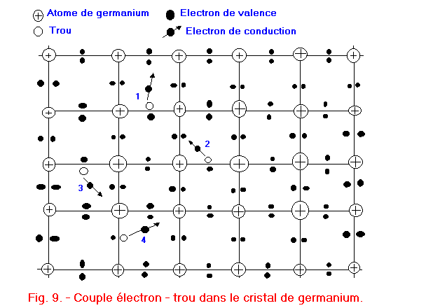
The valence electrons, represented in Figure 9 by black dots ;
The conduction electrons, represented in this same figure by black dots crossed by an arrow.
The valence electrons are those which, while moving from one atom to another, remain connected to the network (as in the case of diamond).
Conduction electrons are those which, during the various displacements, acquire enough energy to break the covalent bonds.
In a very pure crystal, geometrically perfect and maintained at a temperature very close to absolute zero (-
273,16°C), all the electrons of the atoms belong to the category of valence electrons or to use a current expression in physics, belong to the valence band.
By raising the temperature or under the effect of a deformation of the network or by placing the crystal in an intense electric field, a part of the valence electrons gains a certain energy and can free itself from the network, that is to say say go from the valence band to the conduction band. This phenomenon may be more or less important depending on the type of crystal.
At the temperature of 18°C, for diamond, this phenomenon is negligible ; for germanium, an electron over a billion atoms goes from the valence band to the conduction band (an electron over 4 billion valence electrons becomes free).
At first glance, depending on the numbers given, one would think that one in four billion electrons is a negligible quantity. In reality, it must be taken into account that in a cubic centimeter of germanium, there are about 1 x 10²² atoms, which gives about ten thousand billion free electrons. This quantity is therefore more negligible and enough to make the crystal conductive.
But what happens in a crystal where an electron has become free ?
This electron moves in a disordered way in the spaces of the network, unlike the valence electrons that travel the same spaces in well-defined orbits. On the other hand, from the moment when the covalent bond is broken and the electron leaves a free space, a vacuum is created on an orbit.
At a point in the network, there is a hole (also called cavity or gap).
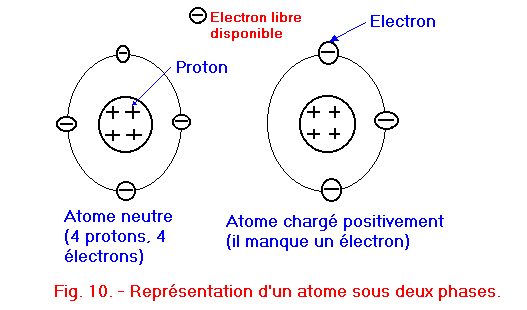
This phenomenon is highlighted in Figure 9 where we can see four free electrons (conduction electrons) and also four holes bearing the numbers 1 - 2 - 3 and 4. The hole represents an electric charge equal to that of the electron but of opposite sign. Indeed, the atom is neutral with all its electrons. If it loses one, this free electron represents an available negative charge ; but the atom is no longer neutral since it has lost an electron ; it thus acquires a positive charge, a charge coming from the protons whose influence is no longer compensated for by the same number of electrons as at the origin. (Figure 10 provides a better understanding of this explanation).
Thus, when in the very pure crystal there are many free electrons, there are so many holes. However, we must not believe that these holes occupy an immutable position. Indeed, as soon as a hole has just been created by leakage of an electron, it is almost instantly occupied by a valence electron. This hole disappears, but does not reform elsewhere in the place left free by the valence electron in question and so on.
We can therefore remember that the holes move from one point to another in the network, unpredictably and disordered like free electrons.
The disordered movement of conduction electrons and holes is the fundamental aspect of electrical conductivity in semiconductors.
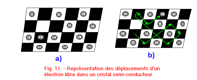
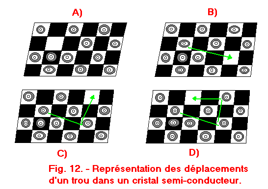
Figures 11 and 12 illustrate the phenomena described above.
The chessboard of Figure 11-a represents the network of a semiconductor crystal. The pions in the white boxes correspond to the valence electrons and the pion of the black box to the conduction electron.
The empty white box represents the hole created by the free electron during its passage from the valence band to the conduction band.
The electron can move freely and disordered in the spaces of the network, just as the pawn in the black box can be moved on the board (Figure 11-b). At the same time, the hole moves in a disordered way ; his career is not as simple as that of the free electron. In fact, for a hole to change position, a valence electron must come to occupy it, leaving a new free hole ; just as to move the free white box of Figure 12-a, it must be occupied by the pawn of another white box.
By repeating this game with other pawns (Figures 12-b, 12-c and 12-d), the free white box seems to walk incoherently across the chess board, just like the holes in the crystal lattice.
In general, the movement of a free electron and a hole do not have a limited duration. Indeed, because of the thermal agitation of all the particles of the crystal, the free electron at a given moment, hits another electron and loses its energy. As a result, he is attracted to a hole that ceases to exist.
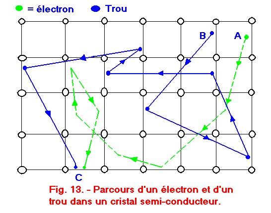
Figure 13 illustrates the path taken by a free electron and a hole.
The electron starts from A and follows, for example, the green dashed path to point C. In principle, it travels along straight paths, changing direction whenever it strikes other particles. As for the hole, starting from the point B and following the line in continuous line, it also arrives at the point C where it disappears, the electron having lost all its energy as a result of the shocks undergone with the particles.
We have just seen so far the very pure and geometrically perfect semi-conducting crystals in which the number of free electrons is exactly equal to the number of holes. These semiconductors are called intrinsic semiconductors.
To use these to make transistors, we must change their structure by appropriate treatment, this is what we will see in the next semiconductor lesson 2.


 Intrinsic semiconductors
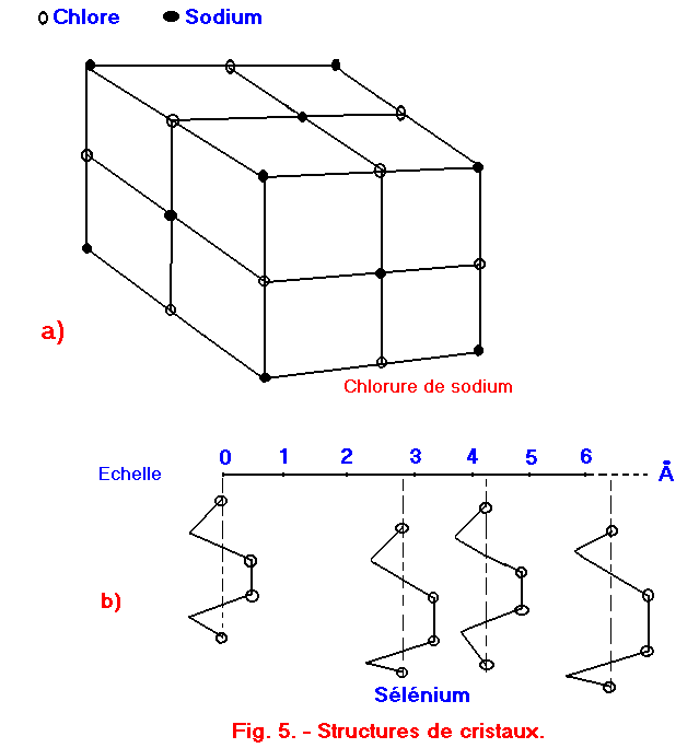
 Click here for the next lesson or in the summary provided for this purpose.
 Top of page
 Next Page