 Astable assembly using two inverters Astable assembly using two inverters
|
Astable realized with the integrated circuit 555
|
Oscillator assemblies using a Quartz
|
| Footer |
Astable Multivibrators Circuits with CI 555 :
3. - ASTABLE MULTIVIBRATORS CIRCUITS WITH CI 555
3. 1. - DEFINITION AND FUNCTION
An oscillator is an electronic circuit that generates a periodic signal. These signals are of two types.
First, there are sinusoidal signals used in radiocommunication techniques. It is the carrier wave of the radio signal and the signal T.V. This type of wave is generated also in the synthesizers of musical notes, in the technology of the radar ...
Then, the second type of signal which interests us more particularly here, is the rectangular signal, specific to the digital technology.
Indeed, this signal is characterized only by transitions from a level H to a level L and vice versa at a frequency determined by the generator circuit. This circuit is generally called astable multivibrator. This circuit has two logical states L and H unstable. The output periodically switches from one logical state to the other complementary state. This is shown in Figure 43.
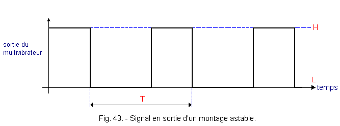
T is the period of the rectangular signal determined by the characteristics of the assembly.
The main function of this signal in logic circuits is to provide a clock usually called clock. This clock is necessary in the synchronous logic circuits where the logical state changes in different points of the circuit are done either at the rising edge or at the falling edge of the clock.
Currently, clock circuits are found in computers, in time measuring devices, in frequency, for data transmission. ....
3. 2. - DIFFERENT MONTAGES OF ASTABLES
We will review a number of multivibratory montages.
3. 2. 1. - ASSEMBLY USING A SCHMITT TRIGGER
Figure 44 shows you an oscillator using a trigger from the CMOS family.
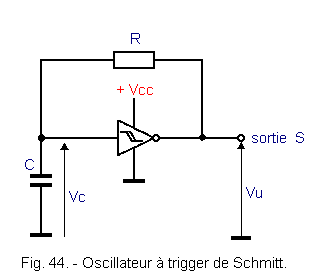
When the assembly is energized, the voltage Vc is zero and the output is therefore at level H.
As it appears in Figure 45, the capacitor C charges through the resistor R and at the instant t1, Vc reaches the threshold VT + of the trigger. The output switches to L : the capacitor begins its discharge through R and at time t2, Vc reaches the only VT- of the trigger..
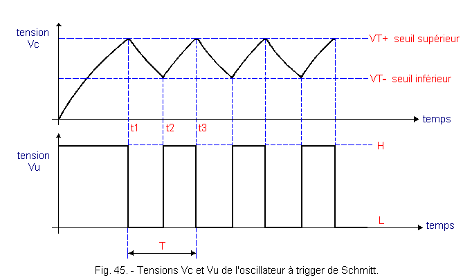
The output goes back to level H and the phenomenon is reproduced indefinitely. The oscillation period T is defined by the relation :
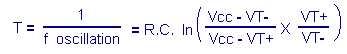
Note :
ln is the symbol of the natural logarithm function. A calculator allows the calculation.
For R = 100 K
W, C = 0,1 µF, Vcc = 5 volts, VT+ = 3,05 volts, VT- = 1,95 volt, we find :T @ 8,9 ms and f oscillation @ 112 Hz.
This assembly is simple but has a disadvantage. Indeed, the thresholds VT + and VT- are a function of the supply voltage Vcc ; this arrangement therefore does not have absolute frequency stability, but may have fluctuations related to variations in the voltage Vcc. For a variation of Vcc from 5 volts to 15 volts, the frequency can vary from 4 to 5%.
Nevertheless, this assembly can be used for applications that do not require great stability and precision.
Moreover, the use of a regulated power supply significantly improves the stability of the oscillator assembly.
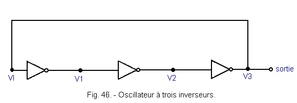
3. 2. 2. - ASSEMBLY USING THREE INVERTERS
This assembly is shown in Figure 46.
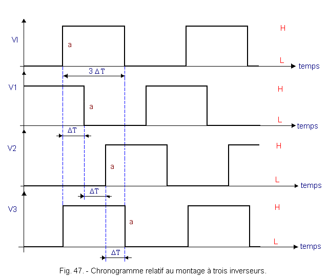
It uses the fact that there is a DT delay for each inverter. The timing diagram shown in Figure 47 allows to understand the operation.
When the signal at point VI (or V3) goes from level L to level H, it is clear that the corresponding output switches after a period of time equal to ΔT. This is so for the three inverters. The letter "a" in Figure 47, shows the evolution of point VI to point V3. Input VI resumes then after 3 ΔT. The period of the signal is 6 ΔT and its frequency This circuit makes it possible to obtain a high frequency oscillator because ΔT propagation times are relatively short. If you want to reduce the frequency of oscillation, just add other inverters. Their number must remain odd.
If n is the number of inverters, the oscillation frequency is 1 / 2nΔT.
With this assembly, the stability is always a function of the supply voltage, the temperature and the load located at its output, therefore the logic circuit that it must drive.
It is possible to improve this assembly by integrating three passive components as shown in Figure 48.
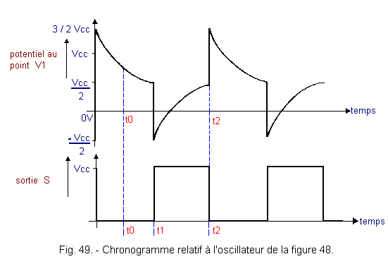
The timing chart for operation is shown in Figure 49.
At time t0, the output S is at the level L and the input of the inverter 1 is at the level H. The potential of the point V1 will therefore decrease and as soon as this potential reaches the switching threshold of the inverter 1 for Vcc / 2, the three inverters will switch to a chain. The output of the inverter 2 goes from the level H to the level L at the moment t1 is a voltage drop of -Vcc and the point V1 is found at the potential (Vcc / 2) -Vcc = -Vcc / 2. However, the output is passed to the level H, so the potential of this point V1 will grow until + Vcc / 2 (time t2) where the three inverters will switch simultaneously. The point V1 is found (Vcc / 2) + Vcc = 3/2 Vcc.
Finally, there is a series of charges and discharges of the capacitor C and each time the point V1 crosses the switching threshold of the inverter 1, the state of the output changes.
As an indication, the oscillation frequency is given by the formula :
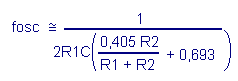
This oscillator is insensitive to the variations of the supply voltage Vcc and its stability in frequency is even better than its frequency is low. Indeed, the frequency depends mainly on the three components R1, R2 and C. This arrangement is presented in Figure 50. The oscillation frequency is given by the formula Moreover, the values of C and R1 should not be too low, because the inverter 2 can not provide a very high output current.
It is always possible to put a variable resistance R1. This adjusts the output frequency of the oscillator.
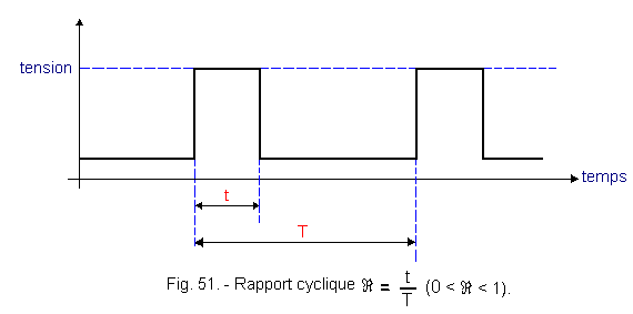
It is also possible to vary the duty cycle R of the rectangular signal.
Figure 51 represents this cyclic ratio R.
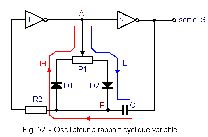
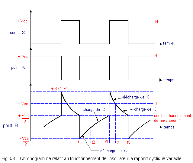
The following assembly shown in Figure 52 makes it possible to vary this cyclic ratio R. The timing diagram in Figure 53 makes it possible to explain the operation of this oscillator. At time t1, the output S is at the level L and the point A at the level H.
The point B is then at the potential -Vcc / 2, as we will see at the end of this reasoning, Vcc being the supply voltage of the assembly.
Capacitor C thus discharges through diode D2 and part of potentiometer P1 since point A is at potential + Vcc and point B at potential -Vcc / 2. At time t2, the capacitor C is completely discharged.
Point B is at potential 0 volt.
The potential of point B continues to increase since point A is always at potential + Vcc.
Capacitor C now charges through the same diode D2 until time t3.
From time t1 to time t3, only diode D2 leads, diode D1 being reverse biased.
It is the same current IL which first discharges the capacitor C and then charges it in a second time.
At time t3, point B is at potential + Vcc / 2, so inverter 1 switches as well as inverter 2.
Point A goes to potential 0 and output S to potential + Vcc.
The potential of the S output has increased instantaneously by + Vcc, so the potential of the B point is similar and thus goes to + 3 / 2 Vcc.
From instant t3 to t5, the same phenomena as those described above are reproduced ; but this time, it is the diode D1 which leads and the diode D2 which is polarized in reverse.
From t3 to t4, the capacitor C discharges, then from t4 to t5, C is charged.
When the potential of the point B arrives at the switching threshold of the inverter + Vcc / 2, the two inverters switch.
The output S which was at + Vcc goes to potential 0 volt, ie a negative edge of -Vcc which is transmitted entirely to point B by capacitor C. This point B which was at a potential of + Vcc / 2 thus passes to :
We have returned to the starting point of our explanation and a new cycle can begin again.
By varying the position of the cursor of the potentiometer P1, the charging and discharging time constants of C (that relating to the period t3 - t1 and that relating to the period t5 - t3) vary.
Thus, the duty cycle R varies.
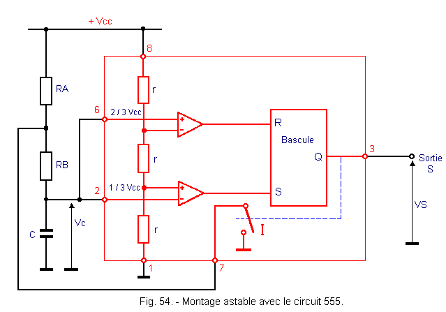
This circuit already used in a pseudo-monostable assembly can be used to constitute an oscillator. His diagram is shown in Figure 54. The switch I is closed when Q is at the L level and open when Q is at the H level, and when the power is turned on.
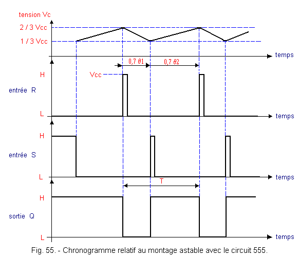
The operation of the oscillator is shown in the form of a timing diagram in Figure 55.
On power-up, the capacitor C charges through the series resistors RA and RB since the switch I is open (Q is at the level H).
The truth table in Figure 56 tells you how the RS flip-flop works.
When the voltage Vc reaches 2 / 3 VDC, the input R goes to the level H, so the output Q goes to the level L. This closes the switch I.
Capacitor C discharges through resistor RB. The discharge constant is equal to θ1 = RB C. When Vc reaches the 1 / 3 VDC threshold, the S input goes to the H level and Q goes back to the H level. The capacitor C recharges with a time constant θ2 = (RA + RB) C and the cycle thus continues indefinitely.
The period T of the rectangular signal, as well as the duty ratio R, are given by the following formulas :
T = 0,7 (2 RB + RA) C
R = (RA + RB) / (RA + 2 RB)
It is therefore possible to vary these two parameters by modifying the respective values of the three components RA, RB and C.
Almost all fixtures seen previously use RC networks.
These mounts may have insufficient stability for some achievements. Quartz oscillators are therefore used when high stability is required for mounting.
This criterion of stability intervenes in clocks measuring the time in which a stability of 10-6, that is 1 second over 13 days, is commonly reached.
In digital circuits working at their limit speed, high stability is also necessary to not exceed the operating standards of integrated circuits.
Another example is provided by microprocessor communications systems where very good stability is required.
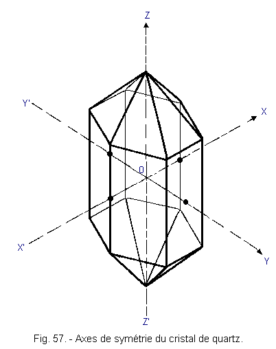
a) Quartz crystals
Quartz is silica (SiO2) crystallized in the hexagonal system.
There are three axes of symmetry in the crystal structure of quartz as shown in Figure 57.
Those are :
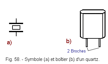
the optical axis ZZ' passing through the vertices. the mechanical axis XX' passing through the edges. the electric axis YY' perpendicular to the faces of the hexagon. In electronics, quartz is represented by the symbol of Figure 58-a.
Figure 58-b shows the appearance of the case commonly used for quartz.
Let's look at their physical properties now.
b) The piezoelectric effect.
In electric oscillators, a quartz slice cut into the crystal is used along one of the axes previously seen.
When an Alternative Voltage is applied to the terminals of this lamella, this lamella deforms and enters mechanical vibration.
It is noted that the amplitude of the mechanical vibrations is maximum for a certain frequency of the Alternative Voltage : this constitutes the resonant frequency of the quartz plate which depends mainly on the axis chosen for the size, the dimensions, and the thickness of this lamella.
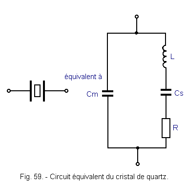
When the quartz crystal is at resonance, it behaves like a tuned circuit that would have the structure shown in Figure 59.
Here are some typical values of the elements of this circuit.
L = 3 H Cs = 0,05 pF Rs = 2 kW Cm = 10 pF The capacity of Cm is due to the mounting (hence its name : mounting capacity) of the quartz blade between two metal frames that form a capacitor.
The series circuit L, Cs, R is the circuit equivalent to the crystal itself. Note the low value of capacitor Cs and, on the other hand, the large value of inductance L compared to those obtained with coils. It is this last characteristic which gives the quartz a factor of quality Q = (Lω) / R very high. This Q factor is usually worth thousands or tens of thousands, while it rarely exceeds 100 in discrete LC circuits. This quality factor makes it possible to obtain quartz oscillators of very good frequency stability.
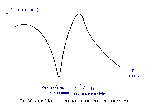
We can define two distinct resonance frequencies for this crystal :
Figure 60 shows the impedance curve of a quartz as a function of the frequency of the signal applied to its terminals.
c) Quartz oscillators.
We can therefore imagine two types of oscillators depending on whether we use series resonance or parallel resonance.
However, the series resonant oscillators are more accurate and more stable because they oscillate rigorously on the frequency of the crystal itself.
On the other hand, oscillators using parallel resonance are dependent on the value of the mounting capacitance Cm and other parasitic capacitances of the arrangement. These, possibly put in parallel on the quartz, can vary the frequency of the oscillator.
It is therefore the first ones we will generally remember for use in logic or microprocessor assemblies.
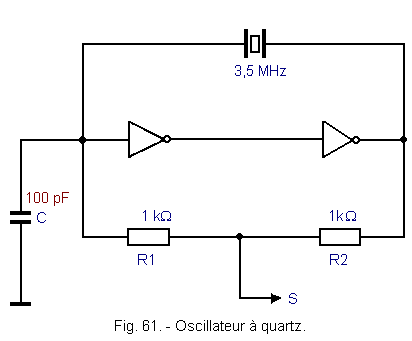
Figure 61 gives a very simple example.
Any oscillator consists of an amplifier and a reaction of the output signal in phase with the input signal.
Here, the two series inverters play the role of a non-inverting amplifier while the reaction is operated by quartz which, at its series resonant frequency, behaves as a simple resistance and therefore provides no phase shift.
Capacitor C and resistors are used to oscillate the start-up arrangement until the quartz resonates.
At the midpoint of the two resistors is taken the rectangular output signal.
This theory ends with this montage using a quartz.
The next theory will be devoted to numerical systems and the different codes used in digital electronics.
Envoyez un courrier électronique à Administrateur Web Société pour toute question ou remarque concernant ce site Web.
Version du site : 10. 4. 12 - Site optimisation 1280 x 1024 pixels - Faculté de Nanterre - Dernière modification : 02 Septembre 2016.
Ce site Web a été Créé le, 14 Mars 1999 et ayant Rénové, en Septembre 2016.
![]() ΔT is expressed in seconds.
ΔT is expressed in seconds.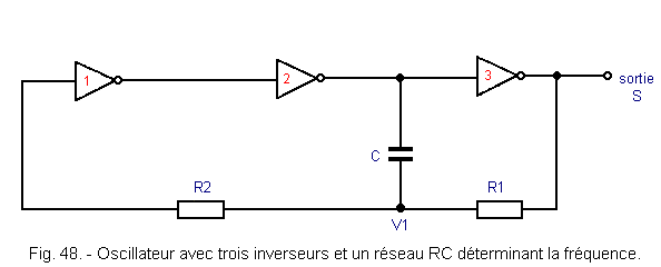
![]() 3. 2. 3. - ASTABLE ASSEMBLY USING TWO INVERTERS
3. 2. 3. - ASTABLE ASSEMBLY USING TWO INVERTERS
![]() .
The value of resistance R2 must be at least ten times greater than that of R1.
.
The value of resistance R2 must be at least ten times greater than that of R1.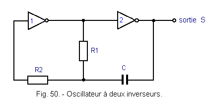
![]() 3. 2. 4. - ASTABLE
REALIZED
WITH THE INTEGRATED CIRCUIT 555 :
3. 2. 4. - ASTABLE
REALIZED
WITH THE INTEGRATED CIRCUIT 555 :
.gif)
![]() 3. 2. 5. - OSCILLATOR MOUNTS USING A
QUARTZ
3. 2. 5. - OSCILLATOR MOUNTS USING A
QUARTZ
![]() the series resonance frequency due to the crystal itself and for which the impedance is minimal because L resonates with Cs.
the series resonance frequency due to the crystal itself and for which the impedance is minimal because L resonates with Cs.![]() the parallel resonance frequency due to the paralleling on the circuit R, L, Cs of the mounting capacitance Cm. For this parallel resonance frequency sometimes incorrectly called self resonance frequency, the impedance at the terminals of the quartz passes a maximum as for any parallel LC circuit.
the parallel resonance frequency due to the paralleling on the circuit R, L, Cs of the mounting capacitance Cm. For this parallel resonance frequency sometimes incorrectly called self resonance frequency, the impedance at the terminals of the quartz passes a maximum as for any parallel LC circuit.
 Click here for the next lesson or in the summary provided for this purpose.
 Top of page
Previous Page
 Next Page
Nombre de pages vues, à partir de cette date : le 27 Décembre 2019
