 Examples of monostable application Examples of monostable application |
Pseudo-monostable |
Pseudo-monostable realized with an integrated circuit of type 555 |
| Footer |
Definition and functions of Monostables :
This new theory will allow you to first examine the monostable circuits, then the Schmitt scales and the oscillators.
These new circuits use concepts of analog electronics (or fundamental), because resistors and capacitors are generally necessary for their operation.
1. - THE MONOSTABLES
1. 1. - DEFINITION AND FUNCTION
In the previous theory, different logical circuits were presented to you. It was basically the slave master D flip-flop and the JK Gold flip-flop, you found that these flip-flops were characterized by two stable states, these flip-flops moving from one state to another under the effect of a command outside the circuit. These latches remain permanently in the state where they are until the control signal makes them switch to the stable state complementary to the previous state.
This is the definition of "bistable" circuits.
In this theory, you will see "monostable" circuits with only one state of stability. Under the effect of an external control, these monostables can pass to the state complementary to the stable state, but invariably recover their state of stability after a time determined by the type of circuit. In fact, these circuits have two complementary logical states, but one is stable, the other is not.
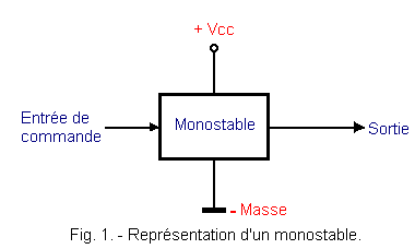
The stable state is the state of rest of the circuit. Figure 1 shows you a simple representation of a monostable.
The logic signals present at the input and output are shown in Figure 2.
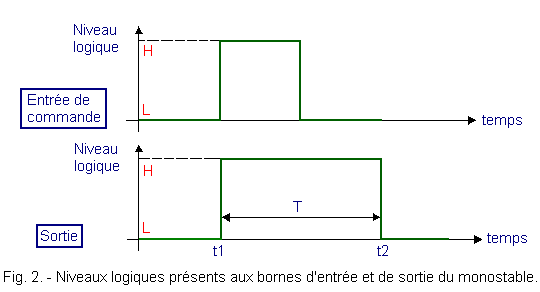
The state of stability of the monostable is characterized by two logical levels L, at the input and at the output of the circuit.
On the other hand, if a voltage step is applied to the input of the circuit at time t1, the output goes to a transient level H which lasts T seconds and falls back to the level L at time t2. It is the fixed duration T which is the fundamental characteristic of the monostable. This duration T is determined by the user according to the application in which the monostable is inserted.
![]() 1. 2. - EXAMPLES OF APPLICATION
1. 2. - EXAMPLES OF APPLICATION
Here are two examples that highlight the usefulness of monostables.
1. 2. 1. - VISUALIZATION CIRCUIT OF A BRIEF IMPULSION
In an electronic set, it may be necessary to visualize a short pulse at a given point in this set.
However, for durations of less than 1/10 of a second, it is impossible to perceive the illumination of an LED. It will be necessary to use a monostable that will play a delaying role by creating a pulse at its output long enough to illuminate a control LED.
Typical assembly is as shown in Figure 3.
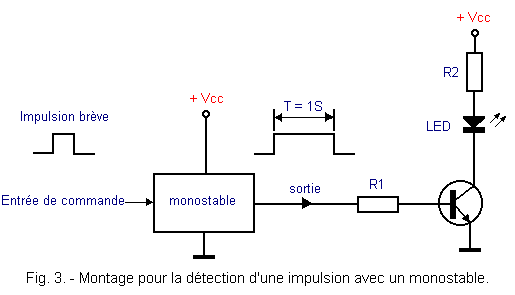
An output pulse of about 1 second is in this case sufficient for the illumination of the LED.
1. 2. 2. - FREQUENCY MEASUREMENT
This application of a monostable circuit makes it possible to measure the frequency of a signal. The block diagram is shown in Figure 4.
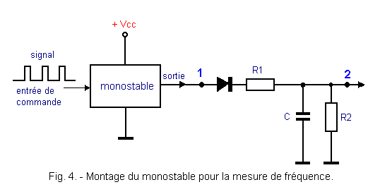
At the entrance of the monostable is applied the signal whose frequency is to be measured.
At the output of the monostable is located a network composed of a diode, a capacitor and two resistors. The two cases A and B shown in Figure 5 make it possible to understand the operation of the circuit.
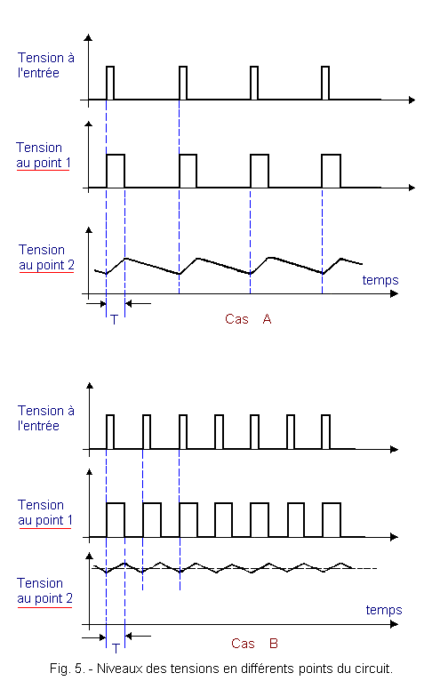
In case A, the signal frequency is relatively low. At each pulse at the input, there corresponds a pulse at point 1 at the output of the monostable.
This pulse allows the charge of the capacitor C through the resistor R1, because the diode is then polarized in the forward direction or passing. The capacitor is charged during the pulse period T, then the voltage at point 1 drops to the low level. The diode is then reverse biased and the capacitor tends to discharge through the resistor R2. The voltage at point 2 is therefore a continuous positive voltage which has a small ripple. It can be likened to a continuous voltage.
In case B, the frequency is much higher. The operation of the circuit is the same as in case A but if the charging time of the capacitor is identical, the discharge time is much shorter.
The capacitor tends to discharge much less than in case A and the voltage at point 2 will be higher than in case A. There is therefore proportionality between the frequency of the signal arriving at the input of the circuit and the DC voltage. that we collect at the output of the circuit. This assembly is therefore a frequency meter or a frequency-voltage converter.
These two examples show the applications that can be made using monostable circuits.
![]() 1. 3. - MONOSTABLE CIRCUITS
1. 3. - MONOSTABLE CIRCUITS
These circuits are subdivided into two categories, first that of the pseudo-monostables, then that of true monostables.
1. 3. 1. - PSEUDO-MONOSTABLES
These different montages require certain conditions to operate in monostable, while true monostables may not meet these conditions.
a) Basic circuit.
This is the circuit shown in Figure 6.
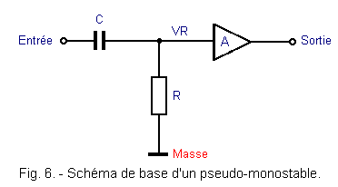
The symbol ![]() designates only an amplifier, that is to say that the output signal varies in the same direction as that present at the point VR.
designates only an amplifier, that is to say that the output signal varies in the same direction as that present at the point VR.
When the input goes from the L level to the H level, the capacitor behaves like a short circuit and the VR point is raised to the H level. Then the capacitor C charges through the resistor R as shown in Figure 7.
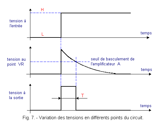
When the voltage at point VR crosses the switching threshold of amplifier A, the output falls back to level L. The duration T is therefore determined solely by the values of R and C. It is approximately 0.7 RC This and valid in CMOS technology.
It should be noted that the input must remain at level H at least as long as the duration of the monostable output pulse. In fact, if the signal present at the input goes back to the level L before the end of this period, the voltage at the point VR would return to a value close to the logic level L and the output would therefore return to the level L. The output pulse would be cut short. It is because of this particular operating condition that this type of circuit is classified as pseudo-monostable.
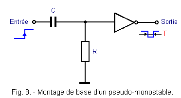
By replacing the amplifier A by an inverter, it is possible to obtain a negative pulse, as indicated in Figure 8.
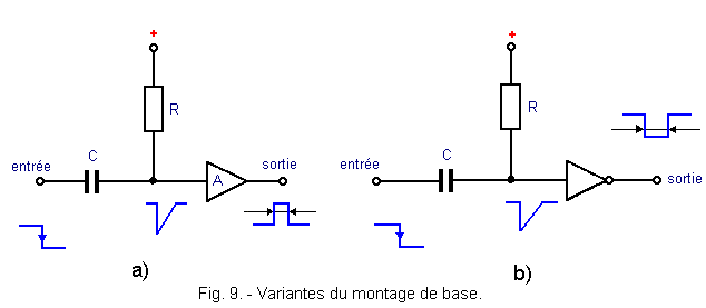
This same type of editing can also be triggered by a transition from a level H to a level L, as shown in Figures 9-a and 9-b.
Another disadvantage of this basic assembly exists.
Indeed, if a new control pulse arrives at the entry of the monostable immediately after that which precedes it, it can occur the following problem illustrated in Figure 10.
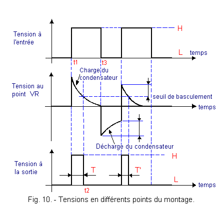
When the input goes back to time t3 at the level L, the voltage at point VR becomes negative because the capacitor is then charged. From t3, the capacitor initiates its discharge. If a new control pulse occurs before its complete discharge, the voltage at point VR does not rise as high as at time t1. The voltage at the point VR will therefore exceed the logic threshold L before the duration T has elapsed. The duration T ' of the output pulse will be less than T. This imposes an additional condition for a correct operation of the monostable.
It is possible to overcome this disadvantage by adding a diode as shown in the assembly of Figure 11.
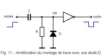
Indeed, at time t3, when the input goes back to the level L, the capacitor C discharges almost instantaneously through the diode D polarized in the forward direction.
The different voltages are shown in Figure 12. The potential at point VR will not fall below -0.6 volts, the voltage threshold of an ordinary silicon diode.
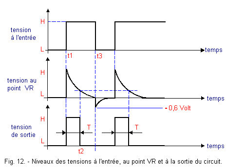
Thus, this assembly will take into account a pulse train very close together.
b) Pseudo-monostable without RC network
For the record, this circuit is shown in Figure 13 because it allows to understand the function of the monostable, but is not used in general in a montage.
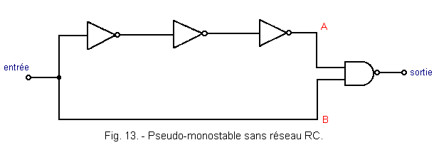
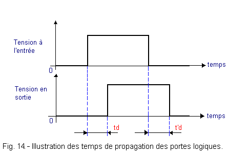
The operation is based on the fact that there is a certain propagation time through any logic gate (NAND, NOR ...). This is illustrated in Figure 14. The times td and t'd may be equal or not.
In the example cited in Figure 13, the shape of the voltages at points A and B and at the output is illustrated in Figure 15.
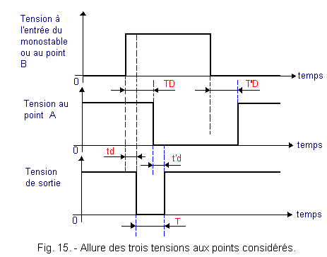
The signal at point A is inverted relative to that at point B at each transition with a delay TD or T'D due to the sum of the propagation times of the three inverters.
Similarly, td and t'd are the signal propagation times through the NAND logic gate.
It is visible in the diagram of Figure 15 that the time constant of this monostable is T substantially at TD. The control pulse must always be of greater duration than the duration T of the output pulse.
![]() c) Pseudo-monostablerealized with a type 555 integrated circuit.
c) Pseudo-monostablerealized with a type 555 integrated circuit.
This integrated circuit is of common use in electronic assemblies. In figure 16, it is mounted in pseudo-monostable (the numbers indicate the pins of the circuit).
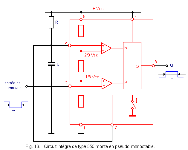
This integrated circuit essentially comprises a voltage divider bridge with three resistors, two comparators symbolized ![]() ,
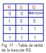
a rocker RS whose truth table is shown in Figure 17, and an electronic switch I.
,
a rocker RS whose truth table is shown in Figure 17, and an electronic switch I.
This switch obeys the following operating rule : it is open when the power is turned on or when the output Q is at level H. When it is at level L, it is closed.
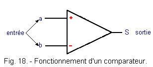
A comparator has essentially two inputs and one output, and operates as shown in Figure 18.
-
Voltage at point "a" greater than that at point "b" → output S at level H.
-
Voltage at point "a" below that of point "b" → output S at level L
The operation of this pseudo-monostable is illustrated in Figure 19.
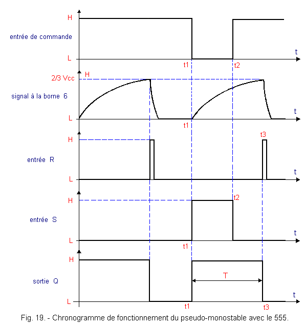
On power-up, I being open, C is charged through R. When the potential at 6 exceeds 2/3 Vcc, the input R of the flip-flop goes to level H.
Output Q goes to L, and I closes. The capacitor is discharged almost instantaneously and the input R goes back to the level L. Since the control input is at the level H, the input S of the rocker is at the level L. So we have R = 0 and S = 0 , the RS rocker is in the memory position. This is the state of rest of the monostable prior to time t1. At this time, the control input goes to L, S goes to H, and Q to H. Since I is now open, the capacitor starts charging. When, at time t3, the input 6 reaches the potential 2/3 Vcc, the input R returns to the level H. Thus, the output Q goes to the level L because the input S is inactive, since it is brought to the level L.
Indeed, the control input is ironed at the level H at time t2 prior to time t3. This is a mandatory condition for proper operation of the assembly, otherwise, at time t3, the two inputs of the flip-flop would be at the level H, so the output Q would be forced to level H.
The duration of the pulse T of this monostable is given by the formula : T = 1.1 RC.
 Click here for the next lesson or in the summary provided for this purpose. Click here for the next lesson or in the summary provided for this purpose. |
 Top of page Top of page |
|
Previous Page |
 Next Page Next Page |
Nombre de pages vues, à partir de cette date : le 27 Décembre 2019

Envoyez un courrier électronique à Administrateur Web Société pour toute question ou remarque concernant ce site Web.
Version du site : 10. 4. 12 - Site optimisation 1280 x 1024 pixels - Faculté de Nanterre - Dernière modification : 02 Septembre 2016.
Ce site Web a été Créé le, 14 Mars 1999 et ayant Rénové, en Septembre 2016.