 Practical achievements of Schmitt's Triggers Practical achievements of Schmitt's Triggers |
Trigger made with NAND doors |
Applications of Schmitt scales
|
| Footer |
Schmitt Flip-Flops and their Applications :
2. - SCHMITT ROCKETS
2. 1. - DEFINITION AND FUNCTION
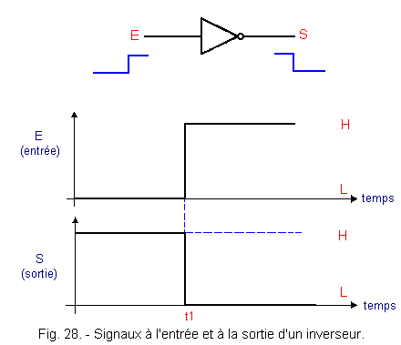
A transition from a logical level L to a logic level H, applied to the input of an inverter, can be shown schematically as shown in Figure 28.
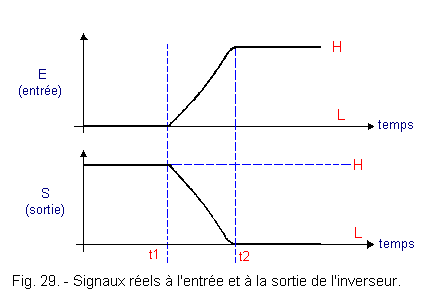
Thus schematized, it appears that the signals present at the input and at the output of the inverter present straight edges, that is to say that the voltage varies instantaneously from a logic state to the complementary logic state. This is a purely theoretical vision. The actual signals move away from this theoretical representation and applied to the same logic circuit, would have the form shown in Figure 29. It thus appears that a logic signal takes a certain time (here t2 - t1) to go from one logical state to another.
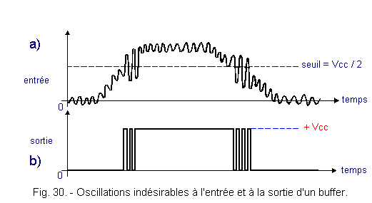
A second remark is necessary. With reference to Figure 30-a, it appears that the voltage has variations due to pests or "noise".
These are defined as small-scale disturbances or voltage variations on an electrical signal.
A buffer can be defined as a current amplifier, that is to say a circuit retaining the shape of the signal and increasing the power available at its output.
This buffer has, for example, a switching threshold equal to Vcc / 2, as shown in Figure 30-a. However, the input signal has disturbances. At the output, the logic signal is not stable but has oscillations as shown in Figure 30-b.
In fact, the undesirable oscillations at the input cross the buffer tipping threshold several times.
It has therefore been necessary to design logic circuits that can overcome these two types of disadvantages.
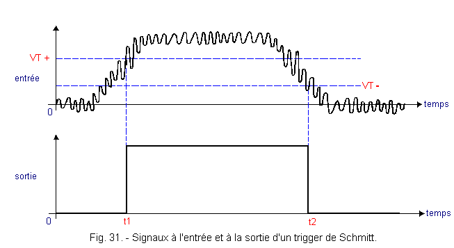
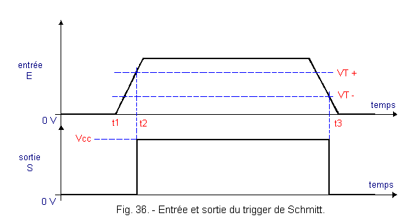
These are the Schmitt scales or Schmitt triggers. The basic idea is to create two switching thresholds, one on the rising edge of a signal, the other on the falling edge of this signal. This is shown in Figure 31. At time t1, the voltage present at the input reaches the switching threshold VT +, the output passes very rapidly from the logic level L to the logic level H, although the threshold VT + is crossed several times during the oscillations present at the trigger input. During the falling edge, it is at time t2 that the input signal crosses the switching threshold VT-. The output then moves very quickly from logic level H to logic level L.
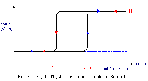
The two moments of changeover are the two moments when the signal crosses for the first time the threshold considered. It is obvious that the more the difference (VT +) - (VT-) is important, the more this circuit will be reliable and insensitive to parasitic fluctuations superimposed on the original signal. This voltage difference between the two thresholds is called hysteresis. This is a characteristic of a Schmitt trigger. The hysteresis cycle is shown in Figure 32.
The arrows in this diagram indicate the direction of travel of the voltages at the input and at the output of the trigger.
It is clear that the output goes from level L to level H as soon as threshold VT + is crossed at the entrance of the rocker (blue arrow). In the same way, the input voltage must go down to VT- so that the output goes from level H to level L (red arrow).
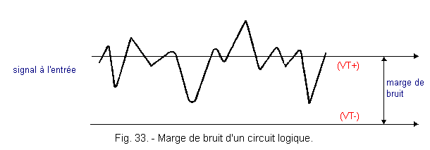
The difference (VT +) - (VT-) is also the "noise margin" which is the voltage difference a signal can have without causing any particular incident on the operation of a circuit. Figure 33 shows the shape of a signal present at the input of a Schmitt trigger.
At one point, the input has crossed the threshold VT +, the output is at level H.
The disturbances of the input signal are visible, but this signal never reaches the threshold VT-, therefore the input is permanently considered in the state H.
The following symbol ( Examples are given in Figure 34. 2. 2. 1. - TRIGGER BASE
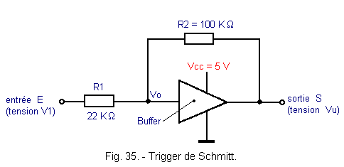
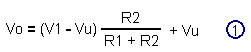
In the trigger of Figure 35, two resistors R1 and R2 are associated with a buffer.
The two resistors are mounted as a voltage divider bridge. The input of the buffer has a very high resistance, of the order of a few tens of MΩ (in CMOS technology). The effect of this buffer will therefore be neglected on the voltage divider bridge. For this, R1 and R2 will have fairly large values. For example, R1 = 22k and R2 = 100kΩ. In this case, we have the relationship Apply to the input E the signal shown in Figure 36.
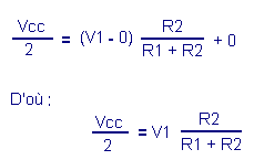
Initially, V1 = Vu = 0 volt. As V1 increases, the input voltage of the buffer Vo also increases and Vu remains zero. Indeed, it is necessary that Vo reaches Vcc / 2 so that the output S switches to level H.
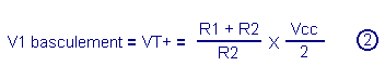
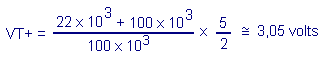
The voltage V1 required for the switching of the buffer is the upper threshold voltage VT +.
Starting from the relation Just before the switchover, the voltage Vo is equal to Vcc / 2 and the output voltage Vu is still zero. Let's replace Vo and Vu by their value in the equation The voltage V1 switching that is called VT + is therefore given by the relation If in this case R1 and R2 are replaced by their value and knowing that the supply voltage is 5 volts, a switching voltage of :
This is the value of the upper threshold.
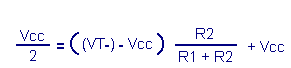
As long as the voltage V1 remains higher than the lower threshold voltage VT-, the output S will remain at the level H (therefore at the voltage Vcc).
When the input voltage V1 goes down again, the buffer switches to the level L for Vo = Vcc / 2.
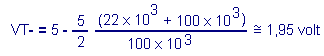
So calculate VT-
using the equation from where :
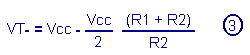
We get the relationship Let's replace R1, R2 and Vcc by their numerical value :
The lower threshold is therefore 1.95 volt.
The hysteresis is (VT +) - (VT-) = 3.05 - 1.95 = 1.1 volts.
It would also be possible to increase the value of the hysteresis by taking a value for R1 greater than 22 kΩ.
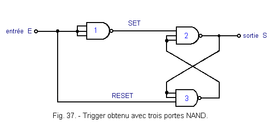
Here, we do not use resistors. This trigger is shown in Figure 37. It includes three three-input NAND gates made in CMOS technology. The operation of this trigger uses the following property : the voltage of the switching threshold is a function of the number of connected inputs together on which the control signal is applied. This threshold will be all the higher as there will be interconnected entries.
In the idle state, the input E and the output S are at the logic level L. When the input voltage increases and reaches VT +, the gate 1 switches, the input SET goes to the level L and the output S at level H.
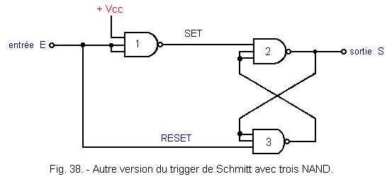
When the voltage at the input E goes down and crosses the threshold VT-, the gate 3 switches and its output goes to the level H. The output S also switches and goes back to the level L. So this assembly is indeed a trigger having two thresholds of switching VT + and VT-. The hysteresis (VT +) - (VT-) is about 1/3 of Vcc or 1.66 volt for Vcc = 5 volts. If you wish to reduce the hysteresis to 1/6 of Vcc, only two inputs of gate 1 must be combined. This is shown in Figure 38.
Thus, the threshold VT + is decreased.
This particular circuit is often used as a Schmitt flip-flop available as an integrated circuit of the CMOS family.
The applications of the Schmitt scales are numerous and some have already been processed. This is the case when it comes to ridding certain rectangular signals of parasites or improving rising or falling edges that vary too slowly.
In chapter 3, the trigger will be presented in an astable montage.
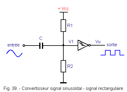
2. 3. 1. - TRANSFORMATION OF SINUSOID TO RECTANGULAR SIGNAL
The assembly is that shown in Figure 39. At the input a sinusoidal signal of frequency F is applied. At the output, a rectangular signal of identical frequency F is obtained. The two resistors R1 and R2 constitute a voltage divider bridge and C is a capacitor used to decouple the input signal from the input of the Schmitt trigger.
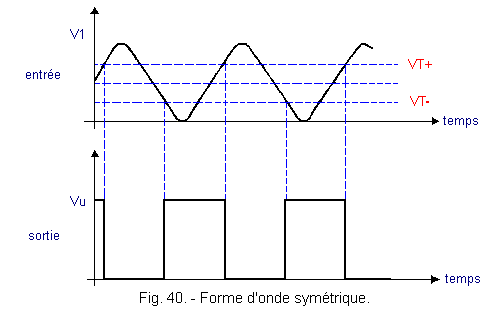
If one wants to obtain a square signal at the output, one will choose to fix a voltage V1 which is equal to (VT +) - (VT-) / 2. This appears clearly in figure 40.
This arrangement can be used to convert a sinusoidal voltage produced by a tachogenerator into a wave train having a frequency proportional to the speed of rotation of the generator.
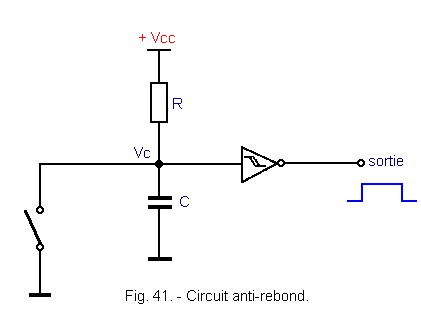
2. 3. 2. - ANTI-REBOUND CIRCUIT
In the assembly shown in Figure 41, it is to deliver a voltage pulse without manifesting a rebound phenomenon at the closure of the contact.
When the switch is closed, there is a bounce of the contacts, but the capacitor C limits the potential variations at the point Vc and the hysteresis of the trigger makes it possible to keep the logic level H at the output.
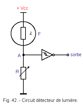
2. 3. 3. - LIGHT DETECTOR
The assembly of Figure 42 makes it possible to detect a certain threshold of light for controlling, for example, the extinction of a lamp.
F is a photosensitive resistor whose value decreases when the light increases. Arrived at a certain threshold of illumination, the point A exceeds the threshold VT + of the Schmitt trigger and the output switches to logic level L.
Even if the light intensity undergoes slight fluctuations, the output remains at level L.
This arrangement also works in the opposite direction. When the light intensity decreases, the point A crosses the potential VT- and the output returns to the level H.
Envoyez un courrier électronique à Administrateur Web Société pour toute question ou remarque concernant ce site Web.
Version du site : 10. 4. 12 - Site optimisation 1280 x 1024 pixels - Faculté de Nanterre - Dernière modification : 02 Septembre 2016.
Ce site Web a été Créé le, 14 Mars 1999 et ayant Rénové, en Septembre 2016.
![]() )
indicates that a logic circuit has a hysteresis cycle.
)
indicates that a logic circuit has a hysteresis cycle.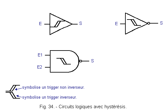
![]() 2. 2. - PRACTICAL ACHIEVEMENTS FROM SCHMITT TRIGGERS
2. 2. - PRACTICAL ACHIEVEMENTS FROM SCHMITT TRIGGERS
![]() following :
following :
![]() preceding, let us express this voltage V1 of tilting.
preceding, let us express this voltage V1 of tilting.
![]() .
.
![]() .
.
![]() by replacing Vo by Vcc / 2 and Vu by Vcc.
by replacing Vo by Vcc / 2 and Vu by Vcc.
![]() :
:
![]() 2. 2. 2. - TRIGGER REALIZED WITH NAND DOORS
2. 2. 2. - TRIGGER REALIZED WITH NAND DOORS
![]() 2. 3. - APPLICATIONS OF SCHMITT ROCKETS
2. 3. - APPLICATIONS OF SCHMITT ROCKETS
 Click here for the next lesson or in the summary provided for this purpose.
 Top of page
Previous Page
 Next Page
Nombre de pages vues, à partir de cette date : le 27 Décembre 2019
