 Footer Footer |
Sum in Parallel with Retention Series - The Summers :
1. 6. - SUM IN PARALLEL WITH RESTRAINT SERIES
Figure 13 shows an 8 bits parallel sum circuit with series hold.
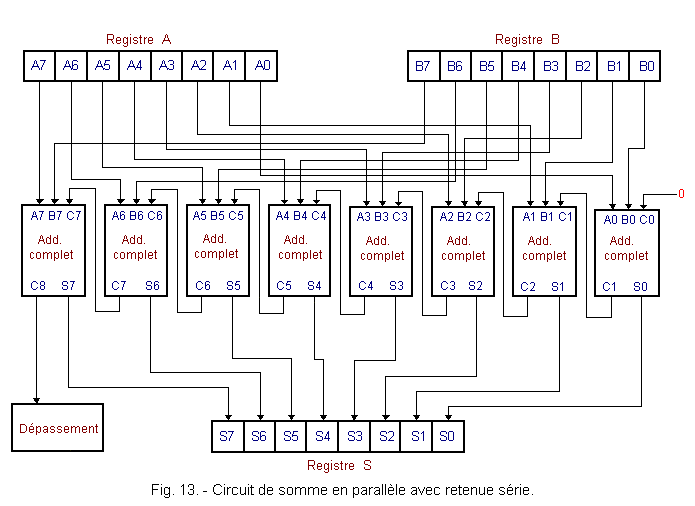
We find that a parallel sum circuit requires as many full adders as there are numbers to add.
On the other hand, since the adopted output of an adder is connected to the input retained by the next, the summing circuit of Figure 13 is said to have a series hold. It should be noted that the selected input C0 of the first adder must be brought to state 0.
The parallel sum method is much faster than the serial sum method and the total time to perform the operation depends essentially on the time required for the carry propagation.
Indeed, even if all digits are summed simultaneously, the hold must propagate from the first to the last adder.
Thus, the result presented on the 8 outputs and on the C8 restraint will only be accurate when this propagation is done.
The mechanism of addition is as follows.
The first summator adds the two digits A0 and B0 and generates the sum S0 and the hold C1.
The second summator adds the numbers A1 and B1 with the hold C1 produced by the first summator. He can not add A1, B1 and C1 only when the retention C1 of the first sum will have been calculated by the first summator.
It is therefore necessary to wait a certain time for the containment to be propagated from floor to floor so that the sum S7 and the retention C8 are established (the sums S0 to S6 will already be established). Before this time, the result contained in S is not necessarily correct.
This mechanism, similar to that found in asynchronous counters, has the same advantage (simplicity of the circuit) and the same disadvantage (slowness).
The sum-in-parallel method with restraint propagation is, however, faster than that of the serial sum.
The time required for a complete adder to calculate the hold is very short, in the case of C-MOS circuits a few tens of nanoseconds.
However, the total time of the addition is the product of this time by the number of digits to be added.
It can not then be neglected especially in computers that must be able to make millions of additions per second. The holdback parallel sum method is used.
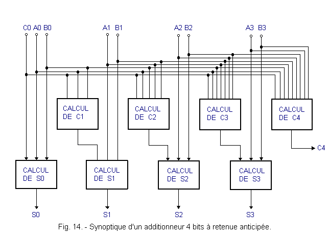
1. 7. - SUM IN PARALLEL WITH ANTICIPATED RETENTION
To sum up more quickly, you have to complicate the previous circuit.
It is based on the fact that the terms of the sum are known and available even before the addition operation begins. We can then calculate, in anticipation, the retention for each floor independently of the previous stages. It is a question of being able to have all the holdings simultaneously and in the shortest possible time.
In other words, the carry C1 must be calculated from the bits A0, B0 and C0, the carry C2 from the bits A0, B0, C0, A1 and B1 and so on.
Figure 14 shows the block diagram of a 4 bits adder with advance hold.
To calculate the deductions in advance, we must transform the equation of the retention Ci + 1 seen previously.
Ci + 1 = Ai![]() iCi
+ AiBi +
iCi
+ AiBi + ![]() iBiCi
iBiCi
Since Ci + 1 worth 1 when Ai = Bi = Ci = 1, we can add the terms AiBiCi to the expression of Ci + 1 as many times as we want (here 2 times).
-
From where Ci + 1 = Ai
 iCi
+ AiBiCi + AiBi +
iCi
+ AiBiCi + AiBi +  iBiCi
+ AiBiCi
iBiCi
+ AiBiCi -
= AiCi (
i
+ Bi) + AiBi + BiCi (i
+ Ai) -
Is Ci + 1 = AiCi + AiBi + BiCi
-
= AiBi + Ci (Ai + Bi)
Posons : product AiBi = pi and sum Ai + Bi = Si
From where Ci + 1 = pi + CiSi
The expression of the restraint of the first floor becomes :
C1 = p0 + C0S0
![]()
and the second floor :
C2 = p1 + C1S1
Replace C1
with its value calculated in ![]() in this expression of C2 :
in this expression of C2 :
-
C2 = p1 + (po + C0S0) S1
-
C2 = p1 + poS1 + C0S0S1

Similarly :
-
C3 = p2 + C2S2
-
= p2 + (p1 + p0S1 + C0S0S1) S2
-
C3 = p2 + p1S2 + p0S1S2 + C0S0S1S2

-
C4 = p3 + C3S3
-
= p3 + (p2 + p1S2 + p0S1S2 + C0S0S1S2) S3
-
C4 = p3 + p2S3 + p1S2S3 + p0S1S2S3 + C0S0S1S2S3

The expressions ![]() ,
,
![]() ,
,
![]() ,
and
,
and ![]() of the holds C1, C2, C3 and
C4 are remarkable by the fact that they claim the same time of computation and that they do not take account of the retention of the previous stage (so no delay due to the spread of the reservoir).
of the holds C1, C2, C3 and
C4 are remarkable by the fact that they claim the same time of computation and that they do not take account of the retention of the previous stage (so no delay due to the spread of the reservoir).
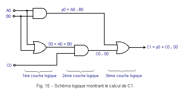
To explain this, let's talk about «logical layer».
A logical layer corresponds to the propagation time of an elementary gate type AND or OR.
For example, the calculation of C1 = p0 + C0S0 requires 3 logical layers as shown in Figure 15.
Although the expressions
![]() ,
,
![]() and
and ![]() retentions C2, C3
and C4 are more complex, they require for their calculation only 3 logical layers
like C1.
retentions C2, C3
and C4 are more complex, they require for their calculation only 3 logical layers
like C1.
We will now see an example of a 4 bits integrated adder with advance hold : the 7483.
Figure 16 shows the pinout and logic diagram of the integrated circuit 7483.
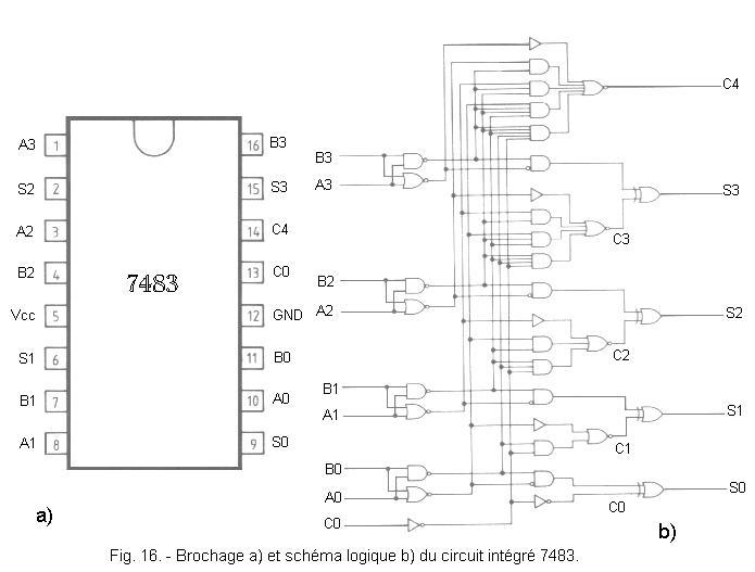
The propagation times of the various inputs to the various outputs of the circuit are collated in the table of Figure 17.
| inputs | outputs | Maximum propagation time (in ns) |
| C0 | Si | 21 |
| Ai or Bi | Si | 24 |
| C0 | C4 | 16 |
| Ai or Bi | C4 | 16 |
With this integrated circuit, 2 numbers of 4 bits are added in 24 ns maximum.
It should be noted that the integrated circuit 74LS83 which is a 4 bits serial-hold adder performs the same operation in 72 ns maximum, or 3 times more.
If one wants to add 2 numbers of more than 4 bits, it is necessary to use several integrated adders and to connect them in cascade.
For example, Figure 18 shows the cascading of two 4 bits adders type 7483 to obtain an 8 bits adder. It is sufficient to connect the output C4 of the first adder to the input C0 of the second.
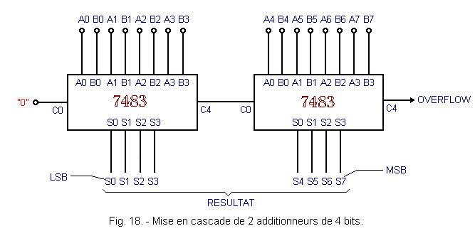
The adder obtained is only partially withholding.
Indeed, we find the mechanism of the series propagation restraint due to the output C4 connected to the input C0.
According to the table of Figure 17, the output C4 of the first 7483 is available after 16 ns. On the other hand, since the outputs S4 to S7 are available 21 ns after the appearance of the C0 of the second 7483, we deduce that the result of the sum of the 2 numbers of 8 bits is available after 16 + 21 = 37 ns maximum.
Each new cascaded adder 7483 adds an extra delay of 21 ns. Thus with 3 circuits 7483, the addition of 2 numbers of 12 bits will require 37 + 21 = 58 ns maximum.
After the adders, let's now examine the comparator circuits.
 Click here for the next lesson or in the summary provided for this purpose. Click here for the next lesson or in the summary provided for this purpose. |
 Top of page Top of page |
|
Previous Page |
 Next Page Next Page |
Nombre de pages vues, à partir de cette date : le 27 Décembre 2019

Envoyez un courrier électronique à Administrateur Web Société pour toute question ou remarque concernant ce site Web.
Version du site : 10. 4. 12 - Site optimisation 1280 x 1024 pixels - Faculté de Nanterre - Dernière modification : 02 Septembre 2016.
Ce site Web a été Créé le, 14 Mars 1999 et ayant Rénové, en Septembre 2016.