 Full Additioner Circuit Displays
The Additioners :
In this theory, we will examine the following combinatorial circuits : adders, comparators, multiplexers and demultiplexers.
1. - THE ADDITIONERS
1. 1. - ADDITION OF TWO BINARY DIGITS
In the binary system, we can represent any number as in the decimal system and we can perform the four elementary arithmetic operations : addition, subtraction, multiplication and division.
As we know, the last three operations can all be reduced to the addition, which is the most important.
We will first recall the addition of two 1-bit binary numbers, we obtain the following 4 sums :
0 + 0 = 0
0 + 1 = 1
1 + 0 = 1
1 + 1 = 10
1st case : the two digits are 0 and the sum is 0.
.gif)
2nd and 3rd case : one digit is 0, the other is 1 : the sum is 1.
.gif)
4th case : The two digits are worth 1 and the sum is worth 10 (= 210).
.gif)
Note that in the first three cases, only one binary digit (or bit) is needed to indicate the result. In the fourth case, two digits are needed : the one on the right is the result (here 0) and the other is the restraint (here 1).
The procedure described is the same as for addition in the decimal system. It differs only in the amount of numbers involved: the two binary digits against the ten decimals.
Figure 1 shows the additions of digits 0 and 1 for both systems.
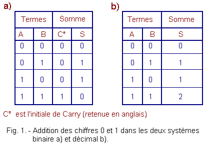
We notice that the results are the same, although in the binary system we must take into account the restraint to express the result two.
1. 2. - ADDITIONAL CIRCUIT
Since we know the rules of the binary addition, we will now see how this operation can be performed by logic circuits.
It is necessary to realize a combinational circuit (Figure 2) whose two inputs A and B and the outputs S and C correspond to the truth table of Figure 1.
Note that S is in state 1 if only one of the inputs is in state 1.
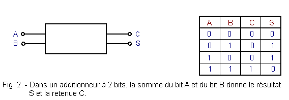
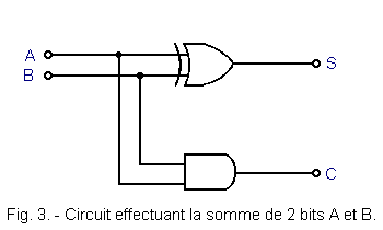
So we are dealing with the logical OR Exclusive function, either :
S = A ![]() B
B
On the other hand, it is noted that C is in state 1 only in the case where A and B are in state 1.
It follows that :
C = A . B
The circuit which performs the sum of two bits can be obtained by associating an Exclusive OR gate and an AND gate as shown in Figure 3.
1. 3. - ADDING BINARY NUMBERS OF SEVERAL DIGITS
The adder circuit discussed above is able to add together two binary numbers of a single digit. For this reason, he is called a half-adder.
Indeed, when one must add numbers of more than one digit, it becomes necessary to have circuits which take into account the retention of the sum made on the figures of rank immediately lower.
To understand this, let's look at how we add two decimal numbers, for example :

This operation is carried out in successive stages : one adds first of all the figures of right, then the following ones by adding the possible restraint.
In a first step, we add 4 and 8, the sum of which is 12 ; we write the result 2 and we retain 1.
.gif)
In the next step, a 3 digits addition must be made because the restraint must be taken into account (here 1). The sum of 7 and 5 plus the deduction 1 gives 13 ; we therefore write 3 and we retain 1.
.gif)
The last step is similar to the previous one : the sum 8 is however without restraint.
The same procedure also applies to binary numbers.
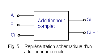
It is therefore necessary to realize a circuit that can add the two figures of the same rank of a binary number with the retention of the previous stage, is three binary digits.
The full adder therefore has three entries, two for terms and one for retention.
Either to sum the two following 8 bits binary numbers :
.gif)
Which gives in decimal code :
.gif)
We start from the last position on the right, where there are two 1. We sum the sum of these two digits according to the table of Figure 1, which gives as result 0 and as holdback 1.
.gif)
In the next step, we must add 3 digits while the table of Figure 1 is limited to the sum of 2 digits.
We will therefore build a table indicating the sum of 3 digits.
With 3 digits, there are 8 possibilities ranging from 0 + 0 + 0 to 1 + 1 + 1.
For each of these possibilities, it is easy to raise the amount.
For example :
-
0 + 0 + 0 = 0 (result 0, retained 0)
-
0 + 1 + 1 = 210 = 10 (result 0, retained 1)
-
1 + 1 + 1 = 310 = 11 (result 1, restraint 1).
The table in Figure 4 summarizes all possible combinations.
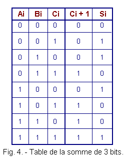
In this table, Ai and Bi are the terms of rank : Ci is the deduction relative to the sum of Ai and Bi ; Ci + 1 is the relative hold on the sum of Ai, Bi and Ci. Si is the result of the sum Ai, Bi and Ci.
Let us now return to the sum taken as an example ; using the table of Figure 4, we obtain for the terms of rank 2 :
1 + 0 + 0 = 1 with a hold equal to 0.
.gif)
If we add up the following figures, we have :
.gif)
And so on until the final result :
.gif)
Let's check the result :
11010110 = (1 x 128) + (1 x 64) + (0 x 32) + (1 x 16) + (0 x 8) + (1 x 4) + (1 x 2) + (0 x 1) = 128 + 64 + 16 + 4 + 2 = 214.
![]() 1. 4. - ADDITIONER CIRCUIT
AND COMPLETE ADDITIONER
1. 4. - ADDITIONER CIRCUIT
AND COMPLETE ADDITIONER
It is therefore necessary to make a circuit that corresponds to the truth table of Figure 4, we obtain the diagram of Figure 5 which shows a complete adder.
Let's now look at the equation of Ci + 1 and Si using the table of Figure 4.
For this, let's draw up the corresponding Karnaugh tables shown in Figure 6.
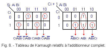
From Karnaugh's first chart, we draw the following Si equation :
-
Si = Ci .
 i
.
i
.  i
+
i
+  i
. i
. Bi + Ci . Ai . Bi + i
. Ai . i
i
. i
. Bi + Ci . Ai . Bi + i
. Ai . i -
= Ci . (
i
. i
+ Ai . Bi) + i
. (i
. Bi + Ai .i) -
= Ci
 + i
. (Ai
+ i
. (Ai  Bi)
Bi) -
= Ci
(Ai
Bi)
In the second table of Karnaugh, We did not search the optimal groupings and this, to be able to highlight the function Ai ![]() Bi already realized with the sum Si.
Bi already realized with the sum Si.
Indeed, the 3 groups indicated give us the following equation of Ci + 1 :
-
Ci + 1 = AiBi +
iBiCi
+ AiiCi -
= AiBi + Ci (
iBi
+ Ai) -
= AiBi + Ci (Ai
Bi)
The two expressions Si and Ci + 1 which have just been calculated, we deduce the logic diagram of a complete adder represented in Figure 7.
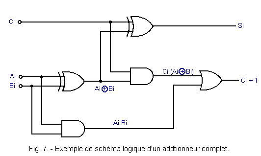
The complete adder is the basic circuit for performing the sum of numbers of several bits.
There are two methods of adding binary numbers.
The first uses a single complete adder to which the numbers of the same rank of the numbers to be added are presented. This is the sum in series.
The second uses as many full adders as there are numbers in the numbers to add. This is the sum in parallel.
![]() 1. 5. - SUM SERIES
1. 5. - SUM SERIES
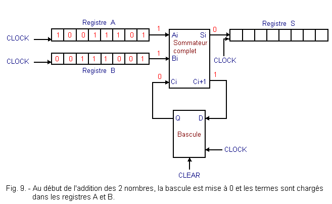
The two numbers (in this case 8 bits) to be added are loaded in two registers A and B as shown in Figure 8. The result of the sum is stored in a third register S. It is also necessary to have a synchronous flip-flop type D which serves to memorize the hold of the previous partial sum.
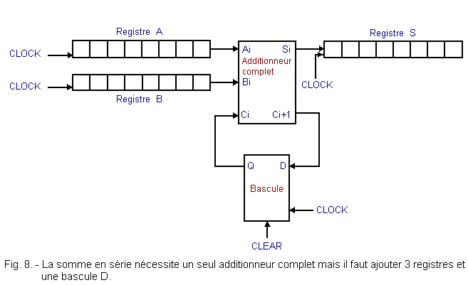
The 3 registers and the flip-flop are controlled by the same clock signal that synchronizes the entire operation.
The operation of the circuit is as follows. Initially, the flip-flop must be set to 0 by activating the CLEAR entry. However, the 3 registers do not need to be reset.
The two terms of the sum are loaded into the registers A and B with a first clock pulse. The first two digits of each term (L.S.B.) are then present at the output of the registers and therefore at the inputs of the adder.
Thus, one finds at the output Si the first partial result and at the output Ci + 1 the first restraint.
The situation is that which appears in Figure 9 where the two numbers of the preceding example are added.
The second clock pulse produces the following facts :
![]() The first partial result is stored in the first stage of the S register.
The first partial result is stored in the first stage of the S register.
![]() The first restraint is stored by the flip-flop.
The first restraint is stored by the flip-flop.
![]() The contents of registers A and B are shifted one stage to the right ; thus the figures of weight immediately higher appear at the inputs of the summator. We are now in the situation of Figure 10. The rocker is now symbolized by a square inside which is inscribed its state.
The contents of registers A and B are shifted one stage to the right ; thus the figures of weight immediately higher appear at the inputs of the summator. We are now in the situation of Figure 10. The rocker is now symbolized by a square inside which is inscribed its state.
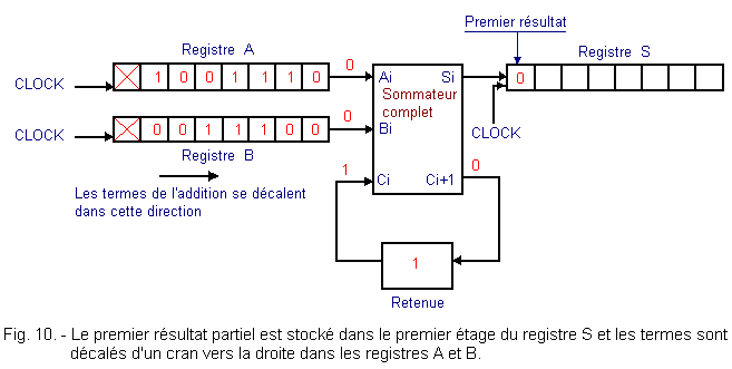
The data present on the serial entry of the registers is not important. The addition proceeds identically for the following figures.
After 9 clock pulses (one for the loading of A and B and 8 for summing), the result of the sum is stored in the register "S" while the output of the latch indicates the hold. We are in the situation of Figure 11.
.gif)
The example addition has the final hold 0, which means that the result 1101 0110 is correct.
If the flip-flop is in state 1, it means that the last sum gave rise to a deduction of 1. It thus exceeds the capacity of the circuit, this is designated by the English term overflow which means to déborder.
There is overflow when the number that is the result of the sum has more bits than those that can be contained in the register (in our case 8).
With 8 bits, the highest number that can be represented is : 1111 11112 = 25510.
With 8 bits registers, we can therefore add numbers between 0 and 255 (expressed in decimal code), but the result of their sum must not itself exceed 255.
Otherwise, we would get a result that, to be stored, would require a 9 bits register.
When using a computer or a summing circuit, it is always necessary to be careful never to exceed the capacity. Overflow gives wrong results. Suppose we make the following sum :
.gif)
The last digit to the left of the result finding no place in the register S is lost. The result that is indicated by the contents of S is 0100 0000, which equals 64 in decimal code and not 320 which is the real result.
To find out if there is an overshoot, it is enough to examine the state of the latch at the end of the addition : if it is in the 0 state, the result is correct ; on the other hand, if it is in state 1, this indicates that there was a deduction of 1 during the last addition and that the capacity of the circuit was exceeded.
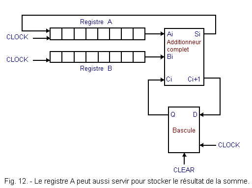
It is possible to save the register S by looping the output S of the adder on the serial input of the register A or B.
If, for example, the output S is connected to the serial input of the register A, as illustrated in Figure 12, the result of the addition will appear in the register A.
Indeed, at each clock pulse, the partial result of each sum is shifted in the register A.
The serial sum method is the closest to our usual way of making additions : adding one digit at a time starting from the one with the lowest weight.
However, it is rather slow because it requires as many clock pulses as there are numbers to add.
For more speed, we use the method of the parallel sum where all the numbers are summed simultaneously.
Depending on the method of calculation of the holding, one distinguishes the sum in parallel with retaining series and the sum in parallel with advance retention.
 Click here for the next lesson or in the summary provided for this purpose. Click here for the next lesson or in the summary provided for this purpose. |
 Top of page Top of page |
|
Previous Page |
 Next Page Next Page |
Nombre de pages vues, à partir de cette date : le 27 Décembre 2019

Envoyez un courrier électronique à Administrateur Web Société pour toute question ou remarque concernant ce site Web.
Version du site : 10. 4. 12 - Site optimisation 1280 x 1024 pixels - Faculté de Nanterre - Dernière modification : 02 Septembre 2016.
Ce site Web a été Créé le, 14 Mars 1999 et ayant Rénové, en Septembre 2016.