In this lesson, we will see several kinds of differential amplifiers with comparators and its environment circuits. The amplifiers were explained at this address (http://www.electronique-et-informatique.fr/Digit/Digit_14TS.php)
but we had less depth in relation to this new lesson, it will be more complex this one.
1 - LINEAR INTEGRATED CIRCUITS
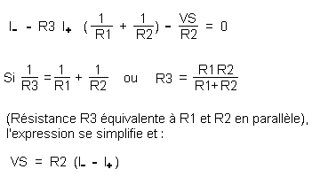
A linear integrated circuit is most often a differential gain amplifier having an output and 2 inputs labeled + and - (symbol of Figure 1). The signal on the + input (non-inverting input) is in phase with that on the output, while the signal on the input - (inverting input) is in phase opposition with the one on the output.
The differential gain calculation is :
DVd,
DVi and
DVs
representing the variations of the input and output voltages. For most amplifiers, you can also write :Gd = Vs / (Vd -Vi); (Vs, Vd, Vi
designating instantaneous voltages at the points considered).
The power of the circuit is made from 2 sources of voltages, one positive Vo, the other negative V'o (of the order of ten volts). There can also be a mass connection.
These last three links are frequently implied in the diagrams.
Such an integrated circuit can be used in two ways :
- only : open loop operation. Because of the large gain of the amplifier, its output is at a fixed high or low level depending on the sign of the potential difference applied between the two differential inputs. The output levels are compatible with the logic levels of the TTL circuits. It is called a comparator. It is a decision element that indicates by a logical output (binary) the result of comparing the amplitudes of two analog quantities.
- with an external network of feedback (linking the output to the inverting input) or reaction network (linking the output to the non-inverting input) : closed loop operation. It is called an operational amplifier.
(An operational amplifier can also generally be used in open loop as a comparator but its output levels are not necessarily compatible with the logic levels of the TTL circuits).
Because of the large gain of the amplifier, the choice of the feedback chain will determine the corresponding transfer function. The introduction of a (positive) feedback chain will cause instability of the system and will allow oscillators to be realized.
1. 1. - COMPARATOR
Definitions.
An ideal comparator presents :
- an infinite differential gain,
- a differential input impedance (between + and -) infinite,
- zero output impedance.
In these conditions :
Vd - Vi > 0 →
Vs at high level, logical output S = 1 (in positive logic),
Vd - Vi < 0 →
Vs at low level, logical output S = 0.
In practice, the number of TTL gates that can be attacked by this signal S represents the fan out of the comparator, the output impedance not being completely zero.
The differential gain Gd is large ( > 50 000) but not infinite. To pass from one level to the other at the output, it is necessary to cause a potential variation DVs
of the order of 2.5 volts in TTL logic and consequently to produce between the inputs + and - a variation of minimum voltage DV
minimale de :DV
= 2,5 / Gd (in volts).
DV
is called the sensitivity of the comparator.
The offset voltage of a comparator is the differential voltage to be applied between the two inputs to bring the output voltage Vs to a given value V which is related to the tilting threshold of a TTL gate and decreases as the temperature increases.
At 25°C ambient temperature V = 1,4 volt.
The amplitude and the rate of change of the input signal affect the response time of the comparator, which it is often advantageous to reduce by offsetting the offset voltage. The rate of change of the input signal in particular causes, taking into account the gain of the comparator, a speed of variation of the output signal which must be sufficient to allow a passage of 0.8 volt at 2 volts in a time of less than 150 nS. This results in a good, non-oscillation switching compatible with TTL circuits.
Naturally, to maintain a good functioning and not to deteriorate the comparator, the input voltages must not exceed certain values (of the order of a few volts to the maximum).
Other characteristics of the comparators (bias current, common mode gains, drifts, etc.) will be defined in the second part of this chapter concerning the operational amplifier, where these characteristics generally play a more important role.
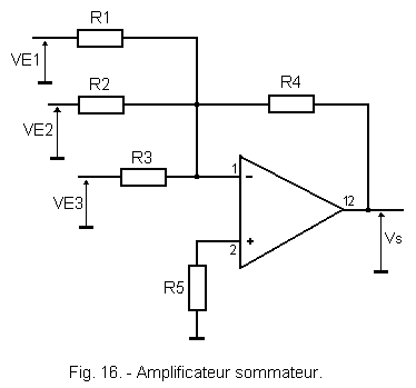
1. 2. - APPLICATIONS.
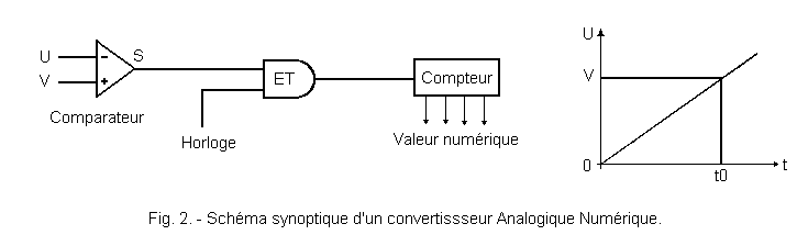
Among many applications we can mention that of analog converters digital (or digital analog).
It is basically the measure of an analog quantity (voltage).
Suppose first the positive voltage. This voltage V is applied to the input + of a comparator whose input - is connected to a voltage generator U in the form of a ramp (Figure 2).
The counter is reset at time t = 0.
As long as U < V, S = 1 and the clock signals, crossing the "AND" Gate, reach the counter.
When U = V, at time t0,
S = 0 and, with the "AND" gate closed, the counter stops. The numerical value that it presents is proportional to t0, thus to V.
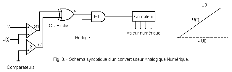
If the voltage V is algebraic, between - U0 and U0, consider a ramp U (t) of pace shown in Figure 3, (in practice the generator provides a periodic sawtooth voltage). This ramp is applied to the inputs - of two comparators.
When U increases from - U0 to + U0, the comparators switch one after the other (1 before 2 if V > 0, which allows to determine the sign of V).
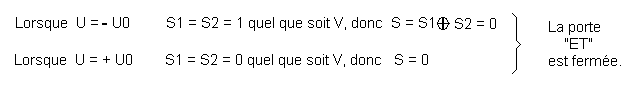
Between these two switches S1 and S2 have complementary values 0 and 1, so S = S1
S2 = 1, which allows the clock signals to reach the counter. The numerical value read on the latter, which corresponds to the time interval separating the tilts of the two comparators, is therefore proportional to the absolute value of the voltage V.
As an ideal comparator, an ideal operational amplifier has infinite differential gain, infinite differential input impedance, and zero output impedance.
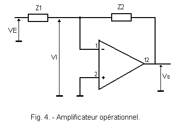
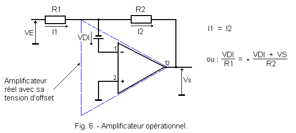
If one carries out with this ideal amplifier, the assembly above (Figure 4), one can write that the currents in Z1 and Z2 are equal, is :
Assuming that VS = 0 when VI = 0, and taking into account the GD = VS / - VI since VD = 0 :
Hence, assuming infinite GD, the transfer function :
The feedback thus applied makes it possible to obtain a transfer function independent of the characteristics of the operational amplifier and linked only to the impedances Z1 and Z2.
Note that finite VS and infinite values of GD result in VI = 0, which precludes direct access to the - input.
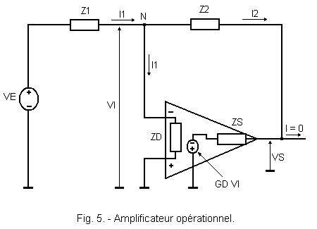
In practice, an operational amplifier will generally present :
-
A differential gain GD greater than 104,
- A differential input impedance ZD of at least 104 W,
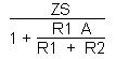
-ZS output impedance of not more than W.
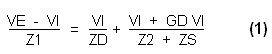
If one wishes to determine their influence on the VS / VE transfer function calculated above, it is necessary to introduce them into the calculation. For that, consider the electric circuit in which they intervene, Figure 5.
The impedance ZD is placed between the + and - inputs.
The operational amplifier then supplies a voltage GD VI represented by an ideal voltage generator (whose polarity takes into account that VI is the voltage on the inverting input) placed in series with the output impedance ZS. The first law of KIRCHHOFF applied to the node N made on the inverting input gives us :
It = I1 + I2.
or :
On the other hand, Ohm's law applied to Z2 and ZS respectively gives us :
b) Static errors.
When the input differential voltage is zero, a very low VS0 output voltage is often observed in practice due to slight asymmetry of the amplifier. It corresponds to the offset or residual voltage at the input (offset voltage) equal to VS0 / GD.
To cancel the output voltage, it is therefore necessary to apply between the two inputs a continuous differential voltage VDI (less than a few millivolts) which compensates for the offset voltage. The influence of the offset voltage on the behavior of the closed-loop operational amplifier can be calculated as follows :
Because the differential input voltage can then be considered as zero due to the very large gain of the amplifier.
from where :
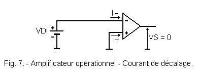
I + and I -.
The offset voltage at the input being compensated, is called input bias current :
(I+ + I-) / 2
The difference | I+ - I-
| = IDI is called offset or residual current at the input (offset current).
These currents hardly exceed a few µA and can be only, for some operational amplifiers, of the order of nA, (1 n A = 10-3 µA).
The influence of the input currents on the behavior of the closed-loop operational amplifier can be calculated as follows :
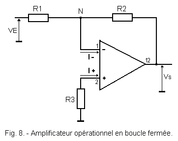
The potential in N is equal to - R3 I+because the differential input voltage can be considered as zero due to the very large gain of the amplifier.
The first law of KIRCHHOFF applied to Node "N" leads us to :
The output voltage is thus proportional to the offset current at the input. These conditions will usually be used to reduce the spurious effect of the input current.
It is always possible to compensate the input offset voltage and current in an operational amplifier, but these quantities depend on the temperature, and the compensation performed at one temperature will no longer be entirely valid for another. The thermal drifts correspond to :
are therefore important to know since they can not usually be compensated for.
They are of the order of a few "µV / °C" for the offset voltage at the input and some p A / °C to some n A / °C (depending on the type of amplifiers) for the current of offset at the input (1 pA = 10-6 µA).
Common mode input voltageVMC
is the arithmetic mean of the voltages VD on the + input and VI on the - input, see : VMC
= (VD + VI) / 2.
The maximum value of VMC
is specified. It is about ± 12 volts.
If the input + is connected to the ground, VD = 0, which implies (see figure 4), VI @
0 and VMC @ 0
By cons, Figure 8, the input + being joined to the ground by a resistor R3, VD =
0, resulting VI @
VD = 0
and VMC =
0.
The output voltage VS of the ideal operational amplifier is zero if the input differential voltage VD - VI = 0, but for a real amplifier we have in this case :
VS = GMC
. VMC (GMC
is the common mode gain).
If an input differential voltage (VD - VI) is then applied, the output voltage becomes : VS = GD (VD - VI) + GMC . VMC
The ratio GD / GMCis the common mode rejection rate (R.M.C)
Expressed in decibels of the order of 70 to 100 dB, it therefore represents the ratio between a common mode input voltage and an input differential voltage that give the same output voltage. In other words, if a voltage VMC
is applied to the inputs, it is the same to apply an equal input voltage differential VMC /
RMC and this voltage has an effect comparable to that of the input offset voltage.
Unfortunately, the common mode rejection ratio is a non-linear function of VMC
voltage and temperature.
A variation DV0
of the supply voltage of the operational amplifier can change the output voltage of DVS.
The ratio of ΔV0 to the ΔVDI variation of the input differential voltage which would produce the same ΔVS variation is referred to as the rejection rate of the supply voltage variations.
DVDI
has an effect comparable to that of the offset voltage at the input.
The rejection rates are of the order of 60 to 100 dB.
A high rate of rejection of supply voltage variations generally makes it possible to use unstable power supplies.
c)
Dynamic errors.
These errors are related to the stability of the closed-loop operational amplifier that we will study.
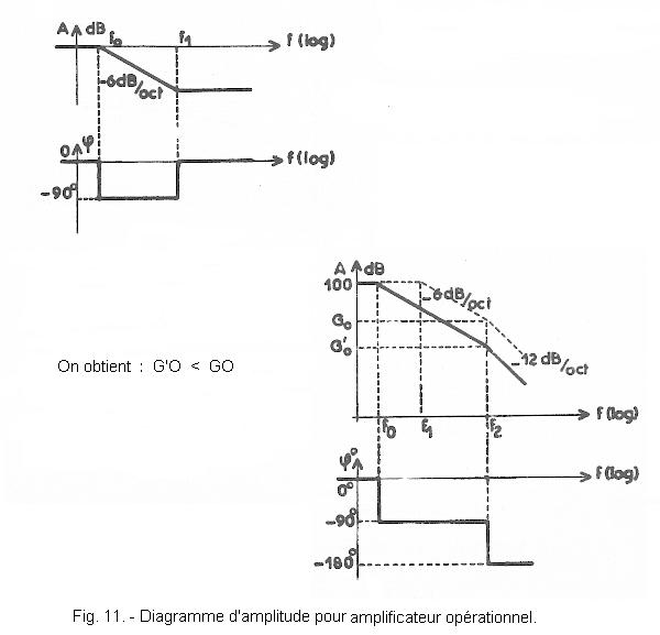
The bandwidth of an ideal operational amplifier in an open and infinite loop, but in reality there are still parasitic capacitances which limit it and lead to an asymptotic Bode diagram for the open-loop frequency response generally having the following appearance :
Closed-loop stability (irrespective of the feedback circuit) can always be determined using the Nyquist criterion by considering the position of the open-loop transfer location with respect to the critical point - 1.
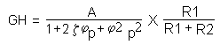
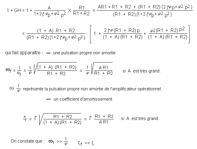
In the very special case in which a feedback is made on the amplifier using two resistors R1 and R2, assuming the differential input impedance of the actual amplifier, the transfer function of the amplifier the feedback chain H is real positive.
It is verified that at low frequency j
= 0 ; the phase shift along the loop is then 180°, since the inverting input is used. But if the frequency of the signal exceeds the frequency f2 of the breakpoint from which the slope of -12 dB / oct appears j approaches - 180° and, given the additional phase shift of - 180°
introduced on the inverting input, the phase shift along the loop makes it to - 360°, which has the consequence of making the amplifier unstable in closed loop, under the usual conditions of use.
To avoid this instability, it is necessary in practice to choose the feedback chain (R1, R2) so that the bandwidth of the closed loop amplifier does not exceed f2 (given a phase margin of the order of 40° still desirable), or introduce correction elements in advance or phase delay between certain points of the amplifier, compensating outputs being provided for this purpose.
The gain G of the closed-loop amplifier (with feedback) being, if GD is very large, 1 /
H = (R1 + R2) / R1, the more we reduce R2, (R1 being constant), the more we will increase the rate of feedback, plus | G | will decrease, and if |
G | < G0 (see Figure 9), the looped amplifier will tend to go into oscillation, its cutoff frequency then being greater than f2.
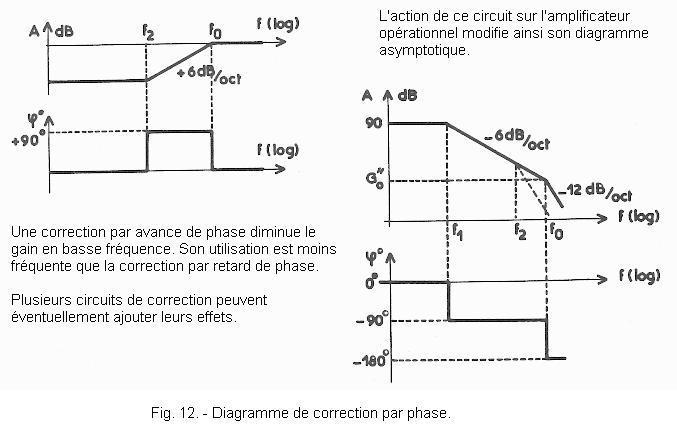
To reduce the value of G0 and thus maintain stability, it is possible to introduce a phase-lag correction circuit corresponding to the following Bode diagram :
The action of this circuit on the operational amplifier thus modifies its asymptotic diagram (Figure 11).
For certain types of operational amplifiers, it is possible by the correction thus introduced to lead to a slope of -6 dB / oct of the amplitude diagram up to a frequency f2 for which G'O = 1 (0 dB) ; under these conditions, even with the maximum rate of feedback, the amplifier will remain stable in closed loop. But this stability is not always the best solution because it causes a sharp reduction in bandwidth and a worse transient response.
If, on the contrary, it is desired to improve the transient response, it will be advantageous to introduce a phase advance corrector corresponding to the following Bode diagram : (Figure 12).
Finally, the operational amplifier with its correctors and its feedback chain will generally behave as a system, either of the first transfer function G (p) = K / (1 + jf
p), or of the second order transfer function G (p) = K / (1
+ 2 zf
jf
p + jf2
p2), where p is the Laplace variable.
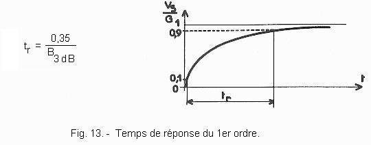
-
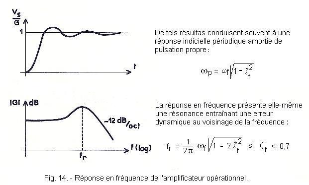
For the 1st order function, we know that the index response is exponential ; the response time (tr) required for the signal to go from 10% to 90% of its final value is given by : (Figure 13).
This 3 dB bandwidth, B3dB,
of the looped system being related to the bandwidth at unity gain B1 of the operational amplifier with unconditional stability by the relation :
B3dB = B1 x (R1 / R1 + R2)
- For the 2nd order function, the rate of the index response depends on the damping coefficient of the looped system.
If the open loop transfer function is :
the denominator of the closed-loop transfer function is :
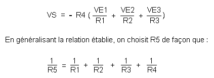
3. - APPLICATIONS.
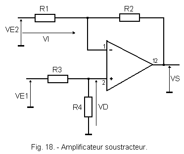
a) Amplifiers.
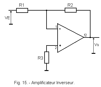
Inverter amplifier.
This arrangement has already been studied (Figure 15).
VS / VE = - (R2 / R1)
We generally taket R3 = (R1 x R2) / R1 + R2)
The current R1 being equal to VE / R1, the input impedance is R1.
It can be shown that the very low output impedance is :
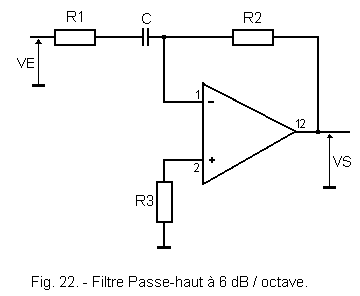
The use of resistive and capacitive elements with operational amplifiers allows the realization of active filters providing a higher energy than passive filters which do not involve amplifiers. The presence of inductance (difficult to achieve for very low frequency signals) can be avoided, and the output of low impedance active filters makes it possible to cascade them very easily.
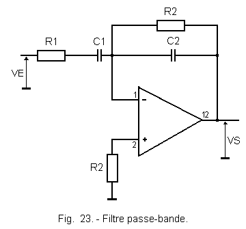
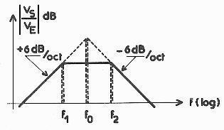
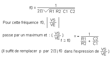
This filter combines the low-pass and high-pass filters just described.
- VE / R1 + (1 / C1p) = VS (1 / R2 + C2 p)
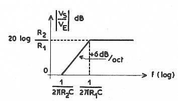
or : VS / VE = (R2 C1 p) / (1 + R1 C1 p) (1 + R2 C2 p)
f1 = 1 (2 P
R1 C1) f2 = 1 (2 P R2 C2)
We take R1 C1
> R2 C2
Which leads to the frequency response below :
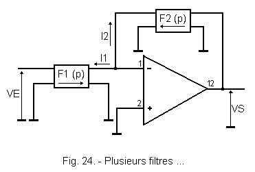
Many other types of filters can be imagined, some of which can be very selective. Indeed, the following editing :
Since the differential input voltage of the operational amplifier is zero, it can be considered that I1 and I2 are short-circuit currents and that F1 (p) and F2 (p) are therefore voltage transfer functions →
short current-circuit. So :
F1 (p) = I1 /
VE
F2 (p) = I2 / VS
Since :
I1 = - I2
VS / VE = - F1 (p) / F2 (p)
The suitable choice of F1 (p) and F2 (p) thus makes it possible to synthesize an active filter.


 Operational Amplifier
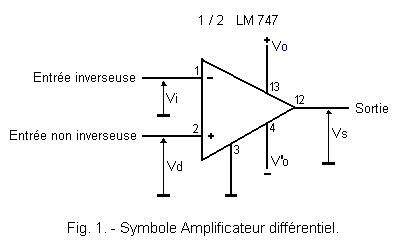
 are therefore important to know since they can not usually be compensated for.
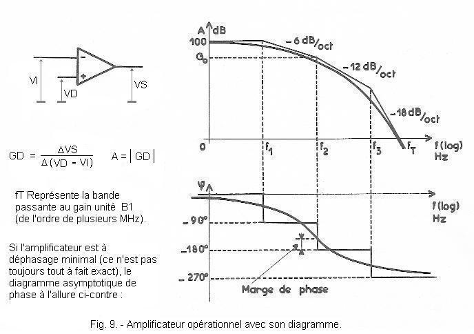

 Click here for the next lesson or in the summary provided for this purpose.
 Top of page
 Next Page