The characteristic curves of a transistor represent the static values that can be determined for any operating point of this transistor.
They are essential because they allow to have a general view on the behavior of the transistor ; in particular, they are very useful for finding the best operating point and therefore for determining the bias circuit. Once the operating point is set, it is often interesting to know the properties of the transistor by limiting itself to this point and operating on numbers instead of continuing to use the characteristic curves.
The properties of a transistor relating to a particular operating point can be defined by means of a number of values called parameters.
The DC amplification coefficient (
and depending on the type of mounting) is a typical parameter, but this is not sufficient to give a complete indication of the properties of a transistor. Indeed, two transistors for example, one of very low power and the other of higher power, can have the same value of amplification coefficient while also having very different characteristics.
To fully determine the properties of a transistor, it is necessary to use several parameters ; more precisely, it takes four for a transistor used in the frequency base, and six when it is a transistor used in high frequency.
There are different parameter systems, that is, the properties of a transistor can be represented in different four-parameter systems. The choice of one or the other system depends only on the type of calculation that must be performed.
In this theory, the different systems will not be analyzed entirely ; we will consider only the most used for low frequency transistors, that is to say the system consisting of the parameters in h.
In addition, some data will be provided on another system, also very used, formed by the parameters in r and also concerning the low frequency transistor.
Finally, some indications will be given on the parameters used in high frequency.
Before considering the meaning of the parameters in h, it is first necessary to define the input resistance and the output resistance of a transistor.
Consider the polarization circuit shown in Figure 1. This circuit makes it possible to adjust the voltage of the collector by means of the potentiometer PC and the base current by the variable resistor RB ; it is thus possible to operate the transistor at any point of its characteristics.
In addition, the VE millivoltmeter and the micro-ammeter IE measure the basic voltage and current (input quantities), while the VS voltmeter and the milliammeter IS measure the collector voltage and current (output quantities).
Let us fix an operating point determined by a certain voltage VCE and a certain current IB. Under these conditions, it flows in the collector circuit a current IC indicated by IS and there exists between the base and the transmitter a voltage VBE indicated by VE.
Then called input resistance relative to the operating point considered and denoted by Re, the value obtained by making the ratio between the voltage and the input current, that is :
Re = VBE / IB
By measuring the voltage VBE in mV (this voltage is very low and it should therefore be expressed in millivolts) and the current IB in µA, the value of Re will be expressed in kΩ.
In the same way, the output resistance is defined as the ratio between the voltage and the output current, see :
Rs = VCE / IC
Since the collector voltage is measured in volts and the current in milliamperes, the output resistance will also be expressed in kΩ.
The resistors Re and Rs thus defined are effectively the resistors presented by the transistor ; Re is the resistance of the base circuit to current IB, and in the same way Rs is the resistance of the collector circuit to current IC, when the transistor is operating at a particular point in its characteristics.
Since these resistors are related to the behavior of the transistor, when only DC bias voltages are applied to its terminals, these resistors are called static resistors (input and output) or DC resistance.
The term "static resistance" indicates that, in the circuit used, no signal to be amplified has been applied to the control electrode (the base, in the case of the common emitter assembly). The transistor is thus in a state of "rest", that is to say in "static".
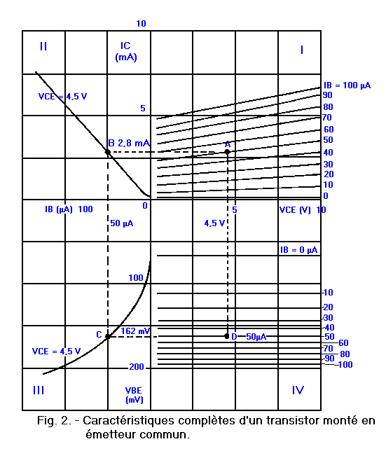
The complete characteristics relating to a transistor mounted as a common emitter are shown in Figure 2.
To determine the values of Re and Rs using them, one must first set an operating point.
Suppose that it is characterized by the following values : VCE = 4.5 V ; IB = 50 µA, it is identified in Figure 2 by a point A on one of the characteristics of quadrant numbered I.
Let's draw a horizontal line through point A and intersect the vertical half-axis. The value of the collector current relative to the operating point is read on the latter : IC = 2.8 mA.
It then becomes possible to calculate the resistance Rs which is equal to :
VCE / IC = 4,5 V / 2,8 mA
1,6 kW
For the calculation of the input resistance, it is necessary to determine the voltage VBE relative to the operating point considered.
To obtain this value, it is first necessary to draw the vertical line passing through point A to meet the characteristic of quadrant IV having as parameter the value of IB relative to the operating point.
In our example, since IB = 50 µA, the curve that interests us is that which has parameter 50 µA ; this determines the point D.
Let's now draw the horizontal passing through the point D and intersecting the vertical axis (point C) ; the value of the voltage VBE, which is 162 mV, can be read on this one.
The value of Re is therefore equal to :
162 mV / 50 µA = 3,24 kW
Point D in quadrant IV and point A in quadrant I both represent the operating point considered ; the only difference is that in quadrant I, we read on the axes the values of the collector voltage and current, while in quadrant IV we also read the collector voltage on the horizontal axis, but on the vertical axis is the base voltage that is read instead of the collector current.
The same operating point can also be represented in quadrants II and III respectively by points B and C. Indeed, these points are both located on the vertical passing through the value IB = 50 µA read on the half axis horizontal left, which means that the transistor has a base bias current of 50 µA ; these points are furthermore located on the characteristics having as parameter the value VCE = 4.5 V, which means that the transistor operates with a collector voltage of 4.5 V.
These values (VCE = 4.5 V and IB = 50 µA) are none other than those of the operating point considered in our example. Since the operating point of the transistor is fixed, it can be concluded that it can be represented by four distinct points, one in each quadrant.
hese in la figure 2 (points (A, B, C, D) are always arranged on the vertices of the corners of a rectangle whose sides (in dotted lines in the figure) intersect the four half-axes according to the values of the four electrical magnitudes. (VCE, IC, VBE, IB) characterizing the operating point under consideration.
It should be noted that, of the four points mentioned, those most appropriate for determining the output and input resistances are respectively the point A and the point C. Indeed, if we draw from point A, the horizontal line and the vertical line up to the points of intersection with the axes, we obtain the values VCE and IC which will be used to determine Rs.
Similarly, if we draw from the point C the horizontal line and the vertical line to the meeting points with the axes, we obtain the values of VBE and IB that we will use to determine Re.
So far, only the common transmitter circuit has been taken into consideration ; however, it is obvious that the same reasoning can be used for common base mounting and in this case too, an input resistance and an output resistance can be determined.
Since for the common base circuit, the input variables are the voltage VEB and the emitter current IE while the output quantities are the base collector voltage VCB and the current IC, we will obviously have :
Re =
VEB /IE
and
Rs = VCB
/IC
These resistances can be determined from the characteristics of the transistor which must now be those of the common base assembly. The procedure to follow is identical to that used for the common transmitter assembly.
2. - ALTERNATING CURRENT INPUT AND OUTPUT RESISTANCE
Consider again the circuit of Figure 1.
Assume that RB and PC have been set to operate the transistor at a certain point in its characteristics and that V'BE, I'B, V'CE and I'C are the values of the indicated voltages and currents. by the devices.
Let us now act on RB so as to increase the basic current I'B up to the value I"B, consequently the base-emitter voltage will also increase and the voltmeter VE will indicate either the value V'BE but a value more big, V"BE.
In other words, we increase the base current of I"B - I'B that we note IB and there is a corresponding increase in the base-emitter voltage V"BE - V'BE noted VBE. Thus, the dynamic input resistance or alternating input resistance is defined as re; its value is :
re = VBE
/IB
It may happen that the increase of IC which is necessarily caused by the increase of IB causes a decrease of the voltage VCE. If this occurs, before reading the values of I"B and V" BE, VCE must be reset to its initial value by acting on PC.
Indeed, the dynamic input resistance must be calculated by keeping the value of the collector voltage VCE constant, and this for the simple reason that this voltage always has some influence on the values of the current and the base voltage.
In a manner similar to that used previously, the PC is now acted on so as to increase the collector voltage by a VCE value by bringing it from the value V'CE to the value V"CE, thereby obtaining an increase in the current of collector and basic current.
If it is desired that the increase of the collector current is not due in part to that of the base current, one must act on RB so as to bring back the base current to its initial value I'B.
The new value I"C can then be read on milliammeter IS and the increase of the collector current is therefore equal to I" C - I'C denoted IC.
We then define the dynamic resistance (or alternating current) output that is designated by rs, its value is :
rs=VCE
/ IC
The name of "AC resistance" or "dynamic resistance" given to the input and output resistances which have just been defined, is due to the fact that these values are those that the transistor presents to the passage of the alternating current (superimposed to the DC bias current) constituting the signal to be amplified applied to the input of the transistor or amplified taken at the output.
It is interesting to note that the transistor behaves very differently with respect to the DC bias current and the AC current constituting the signal.
Also, the values ??of the DC and AC resistances are generally very different from each other.
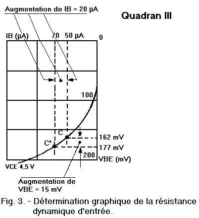
To get an idea of the difference between these values, it is necessary to calculate re and rs for the operating point considered in the previous example.
For the determination of re, it is necessary to cause an increase of IB and to see what increase of the voltage VBE results therefrom (while of course keeping the value of the collector voltage constant).
Referring to the input characteristic (quadrant III) of figure 2, it can be seen that the operating point C must move on the curve having for parameter 4.5 V (since this is the value of the voltage collector relative to the operating point considered).
Suppose that the base current is increased from 50 µA to 70 µA : the operating point changes from C to C' as shown in Figure 3. As a result, the VBE voltage increases from 162 mV to 177 mV.
The value of re relative to the operating point C is therefore equal to :
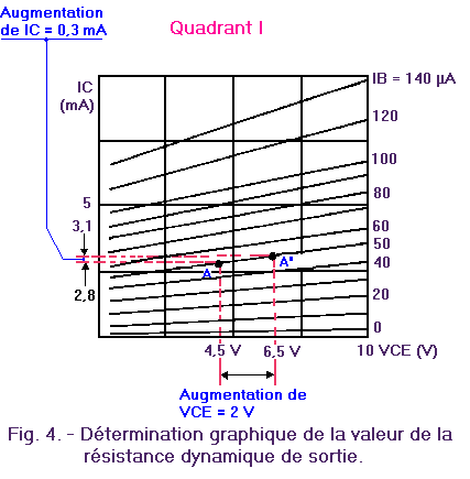
Similarly, the dynamic output resistance can be determined from the characteristics shown in quadrant I shown in Figure 4 below.
Assume that the collector voltage is increased from 4.5V to 6.5V by keeping the value of the base current constant ; the operating point of the transistor then goes from A to A'. Point A' is also on the characteristic having as parameter IB = 50 µA (see Figure 4 below).
This increase in VCE shifts the collector current from 2.8 mA to 3.1 mA as can be read on the vertical scale of Figure 4. Therefore, the value of the dynamic output resistance is deduced :
rs = VCE
/ IC
= (6,5 - 4,5) / (3,1 - 2,8) = 2 V / 0,3 mA
6,67 kW
As can be seen by comparing the results obtained with those of the previous example, the transistor, although operating at the same point of its characteristics, exhibits DC input and output resistance values which are very different from those presented. alternating current.
Indeed, the input resistance is higher in the first case (3.24 kΩ against 0.75 kΩ) while in the second case the output resistance increases significantly (1.6 kΩ).
In the common base arrangement, it is likewise possible to define a dynamic input and output resistance.
Their value can be determined graphically using the characteristics of the common base mount transistor or experimentally by measuring the current and voltage increases on the common base circuit.
In a circuit of this type, the input quantities are represented by the emitter-base voltage VEB and the emitter current IE while the output quantities are given by the collector-base voltage VCB and the current IC.
We deduce the following formulas :
Re = VEB / IE
; re = VEB
/ IE
; Rs = VCB / IC ; rs = VCB
/ IC
Hybrid parameters (symbolized by the letter "h") are four in number for transistors used at low frequency.
To distinguish these parameters, two-digit indices are used. The four parameters are then identified as follows : h11, h12, h21, h22.
The hybrid parameters correspond to the type of editing used. Thus, those relating to the common transmitter assembly, those relating to the common base assembly and those relating to the common collector assembly are distinguished. It is thus necessary to be able to differentiate them to know to which type of assembly they relate.
For this reason, the index is completed by the letter "e" in the case of the common transmitter assembly, by the letter "b" in the case of the common base assembly and by the letter "c" in the case of the common header assembly, hence the symbols :
h11e ; h12e
; h21e ; h22e (common issuer),
h11b ; h12b
; h21b ; h22b (common base),
h11c ; h12c
; h21c ; h22c (common collector).
The definition of each parameter and the way to deduce the values are identical for the three types of assembly. For simplicity, we will limit ourselves to the case of the common transmitter assembly.
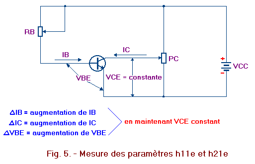
Let's make a small increase to the current IB making sure that the value of the collector voltage remains constant (by retouching PC, if necessary). Let's call IB
the value of this increase. Similarly, let VBE
denote the corresponding increase of the base voltage and by IC
the increase of the collector current. These ratings are shown in Figure 5.
The parameters h11e and h21e are defined by the following formulas :
h11e =VBE
/ IB
at VCE constant
h21e =IC
/ IB at VCE constant
We can see immediately what these parameters indicate or more precisely what is their physical meaning ?
The parameter h11e is none other than the AC input resistance. Indeed, its value is given by the ratio between the increase of VBE and the increase of IB at constant collector voltage ; it is defined in the same way as was the input resistance in the previous paragraph. The value of h11e is therefore expressed in Ω (or in kΩ) since it is a resistance.
The parameter h21e, on the other hand, represents the ratio between the increase of the collector current and the increase of the basic current with constant collector voltage. This is the AC amplification coefficient. Since the characteristics represented in quadrant II are comparable to lines passing through the origin, it is considered that the DC amplification coefficient
and the AC amplification coefficient h21e are equal.
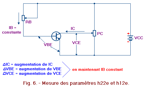
To determine the other parameters h, consider again the diagram of Figure 1. Let us increase the collector voltage by acting on PC, without forgetting to retouch RB to bring IB back to its initial value.
denotes by
VCE,
IC
and VBE,
respectively, the increase of the collector voltage and the consequent increases for the collector current and the base voltage, as shown in Figure 6.
The values of h22e and 12e are given by the following formulas :
h22e = IC
/ VCE
at IB constant
h12e =VBE
/VCE
at IB constant
It is noted that the parameter h22e is the ratio between the increase of the collector current and the increase of the constant base current collector voltage, that is to say the inverse of the AC output resistance.
The inverse of the resistance being defined by the conductance, the parameter h22e therefore represents the AC output conductance of the transistor ; its value is expressed in units of conductance, that is to say in siemens (S) or millisiemens (mS) or in microsiemens (µS), but it is most often given in mA / V (milliampere by volt), unit equivalent to millisiemens or µA / V (equivalent to µS).
Finally, the parameter h12e is given by the ratio between the increase of the base voltage and that of the collector voltage which caused it (at constant basic current). This parameter is called the voltage response coefficient, since it expresses the influence of the output voltage on the input voltage.
Generally, the input voltage is only slightly influenced by the output voltage, that is the increase of VBE
Using the same reasoning, but this time for a common basic circuit, we can define the hybrid parameters h11b, h21b, h12b, h22b. Here, however, the parameter h21b is substantially equal to the coefficient
.
In conclusion, let's see the definition that can be given to the different parameters :
h11 =
Input resistance,
h21 =
Current amplification coefficient,
h12 =
Coefficient of reaction in tension,
h22
= Output conductance.
It is important to remember that the first two parameters must be measured by keeping the output voltage constant, while the other two must be measured at constant input current.
It should be noted that the symbol h (initial of the hybrid term) attributed to these parameters is due to the fact that they are not homogeneous as regards their units of measurement. Indeed, while two of them (h21 and h12) are pure numbers and therefore dimensionless, the first (h11) is a resistance and the last (h22) a conductance.
By observing the formulas that define the various hybrid parameters, we note that the number 1 refers to the input and the number 2 to the output. Thus, h11 indicates the parameter obtained by the ratio of two input quantities. Similarly, h21, h12 and h22 respectively indicate the parameters obtained by the ratio of an output quantity with an input quantity, an input quantity with an output quantity and finally between two output quantities.
There are also other terms for defining parameter indices. Indeed, h11 is sometimes referred to as hi because it represents the input resistance ("i" being the input initial = input).
The parameter h21 is also denoted by hf because it represents the direct amplification, that is to say the amplification that a current "going from the input to the "output" undergoes ("f" being the initial of forward = direct).
The parameter h12 can be replaced by hr because it expresses a reaction in the "opposite" direction ("r" being the initial of reverse = inverse), that is to say between the output and input voltages.
Finally, the parameter h22 can be replaced by ho because it represents the conductance of "output" ("o" being the initial of output = output).
The properties of a transistor depend to a greater or lesser extent on its operating point.
It is therefore obvious that the hybrid parameters will also depend on the operating point, that is, they will vary when moved to the feature.
For this reason, when indicating the values of the parameters h, it is necessary to specify to which operating point they relate.
In the case of transistor BC 108B for example, the parameters h given for a common emitter assembly (operating point : VCE = 5 V and IC = 2 mA at the frequency of 1 kHz and at a temperature of 25° C.) are the following :
h11e =
hie = 4,8 kW,
h21e = hfe = 330,
h12e = hre = 0,0002,
h22e = hoe =
30 µA / V.
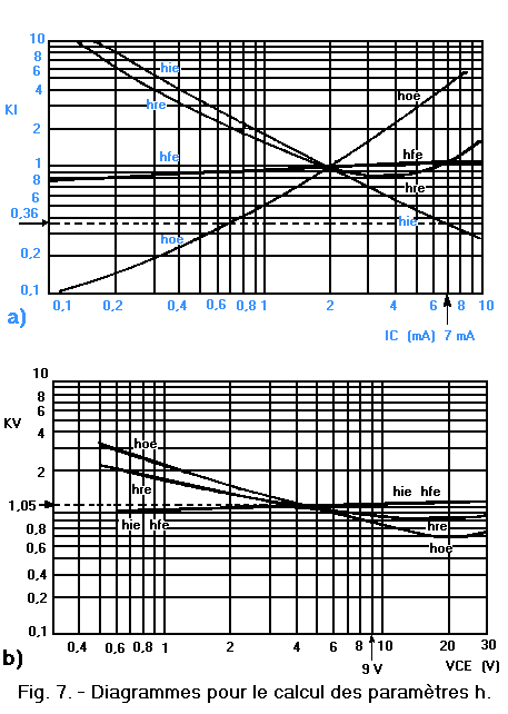
For hybrid parameter values for operating points different from the one for which the values were given, appropriate diagrams found in the manufacturer's manuals should be used. An example of these graphs is shown in Figure 7 ; they are relative to the transistor BC 108B and are used to move from the point characterized by VCE = 5 V and IC = 2 mA at any point in the permitted area of the characteristics of the transistor in question.
The diagram in Figure 7-a below takes into account the current IC of the new operating point, while that of Figure 7-b is related to the voltage VCE.
Suppose that we want to calculate the parameters h of transistor BC 108B for the operating point characterized by VCE = 9 V and IC = 7 mA. The curve hie of Figure 7-a gives us for IC = 7 mA the value KI = 0.36 while that of Figure 7-b gives for VCE = 9 V the value KV = 1.05.
The relative h'ie value at the operating point level is obtained by the following formula in which hie is the value relative to the initial operating point :
h'ie = hie x KI x KV = 4,8 x 0,36 x 1,05 = 1,81 kW
By doing the same for the other parameters, we find the following values :
For hfe : KI = 1,1 ; KV = 1,05 so h'fe
= 330 x 1,1 x 1,05 = 381
For hre :
KI = 1,15 ; KV = 0,87 so h're = 0,0002 x 1,15 x 0,87
0,00020
For hoe :
KI = 4,6 ; KV = 0,79 so h'oe = 30 x 4,6 x 0,79 = 109 µA / V
Although the diagrams of Figure 7 relate to transistor BC 108B, they can nevertheless give an idea of the variation of the hybrid parameters relating to the common emitter assembly for any type of low power transistor used at low frequencies, when the current and the collector voltage vary.
By observing the diagram of Figure 7-a, it can be said that, as IC increases, the input resistance of the transistor (hie) decreases substantially ; on the other hand, the output conductance (hoe) increases considerably and since the conductance is the inverse of the resistance, it is deduced that the output resistance decreases sharply as the collector current increases. The coefficient of amplification in current hfe remains, meanwhile, substantially constant.
Similarly, by observing the diagram of Figure 7-b, it can be said that the input resistance (hie) and the coefficient (hfe) remain substantially constant when the collector voltage increases, while the output conductance decreases slightly, which means that the output resistance increases slightly.
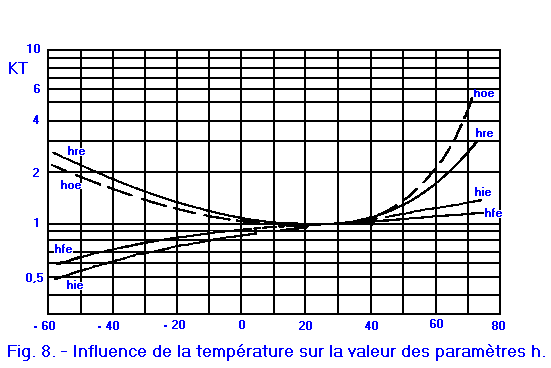
5. - INFLUENCE OF TEMPERATURE ON THE VALUE OF HYBRID PARAMETERS
Hybrid parameters, like characteristics, vary when the temperature at which the transistor is located (or better its junctions) varies. The values indicated in the manuals are, in general, relative to the temperature of 25° C.
To know the new values that the hybrid parameters take when the temperature changes, one can refer to Figure 8 which represents a diagram similar to those of figure 7. This one gives the coefficient KT by which one must multiply the values of the parameters h, relative to the temperature of 25° C, to switch to those relating to another temperature between -60° C and + 80° C, for low power transistors used at low frequencies.
The diagram of Figure 8 shows that above 25° C, all parameters increase with temperature, the input resistance and the amplification coefficient increasing less rapidly than the output conductance and the coefficient of reaction.
For example, by raising the temperature from 25° C to 70° C, the output conductance becomes four and a half times greater, which means that the output resistance becomes four and a half times lower, while the hfe coefficient on the other hand, only 1.1 times bigger.
Below 25° C, the input resistance and the amplification coefficient gradually decreases with temperature, while the output conductance and the reaction coefficient start to grow again. The hfe coefficient, for example, is reduced by 22% at the temperature of -25° C.
6. - DETERMINING
PARAMETERS "h" FROM CHARACTERISTICS
The value of the parameters h can be determined from the families of characteristics of the transistor, obviously considering the point of operation which interests us.
To calculate the value of the hie parameter, the procedure to be followed is the same as that shown in Figure 3 since, as we have seen, this parameter coincides with the AC input resistance.
To determine the hoe parameter, the procedure is analogous to that shown in Figure 4, with the difference that the increase in the collector current and the collector voltage must be compared, since this parameter coincides with the opposite the output resistance.
The hfe parameter is determined from the characteristics of quadrant II. It suffices to take an increase in the collector current in correspondence with the increase in the base current when the collector voltage remains constant.
Finally, there remains the calculation of the parameter hre. In this regard, it should be noted that this parameter is very difficult to determine on the characteristics of quadrant IV because of its generally low value.
End of this first lesson and to finish this one, we will continue on another page entitled "Semiconductors 6 - 2nd part". (Paragraph 17.1 See basic electronic summary).


 DC input and output resistance
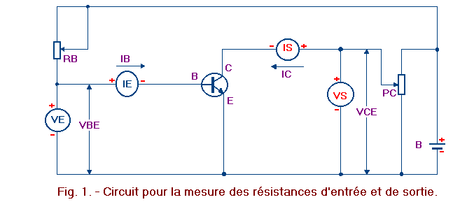
 Click here for the next lesson or in the summary provided for this purpose.
 Top of page
 Next Page