 Universal Registry Universal Registry |
Analysis of a Universal Integrated Register : 74 194 |
Dynamic Registry |
| Footer |
Bidirectional and Universal Registers - Dynamic Register :
6. - BIDIRECTIONAL REGISTER
6. 1. - PARALLEL REGISTER - SYNCHRONOUS SERIES WIRED FOR LEFT SHIFT
Synchronous loading parallel-serial register allowed to preposition its content, then to make a shift to the right of it thanks to the command entry SHIFT / LOAD.
The information was shifted from the Q1 output to the Q4 output.
It is sometimes useful to be able to shift the information in a register in the other direction, that is to say from the output Q4 to the output Q1.
This is the shift to the left.
Let's see what are the links to perform on the registry to get the left shift of its content.
Connect the Q4 output to the E3 input, the Q3 output to the E2 input and the Q2 output to the E1 input.
We thus come to the diagram of Figure 30.
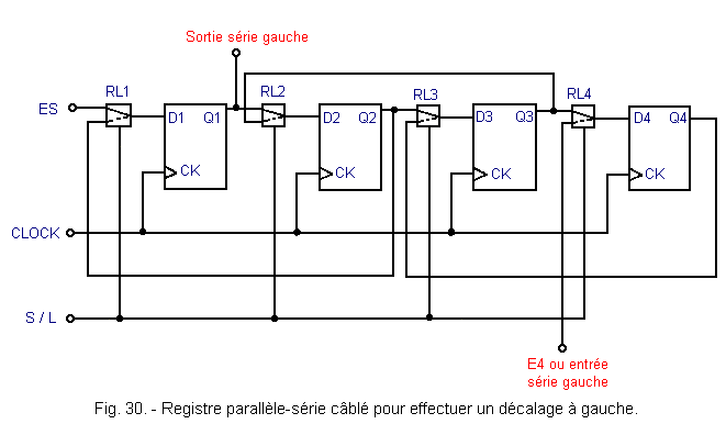
Let's take the SHIFT / LOAD (S / L) input to the H level. Thus, at the same time, the E4 input is «connected» to the D4 input, the Q4 output to the D3 input, the Q3 output at the D2 input and the Q2 output at the D1 input.
Now, if we enter the information through the input E4, they will shift at each clock pulse from the output Q4 to the output Q1. We are witnessing the shift to the left of the information. Input E4 becomes the left serial input and output Q1 the left serial output.
Figure 31 shows the equivalent circuit diagram obtained.
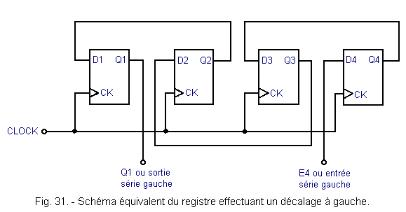
If, on the other hand, the input SHIFT / LOAD is brought to the level L, we obtain a shift to the right of the contents of the register.
The ES input is the right serial input of the register and the Q4 output is the right serial output.
In summary, the examined register operates either in right shift mode or in left shift mode.
Only, it no longer works in LOAD mode.
To obtain the three operating modes mentioned above, the universal register must be used.
![]() 6. 2. - UNIVERSAL REGISTER
6. 2. - UNIVERSAL REGISTER
6. 2. 1. - SCHEME AND EXAMINATION OF THE FOUR OPERATING MODES
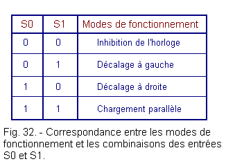
To differentiate between the following three modes, parallel load, right shift, left shift, two control inputs are required.
These, called S0 and S1, make it possible to differentiate four modes of operation. However, three modes are provided. The fourth will inhibit the action of the clock.
The table in Figure 32 indicates the correspondence between each of the operating modes and each of the combinations of the inputs S0 and S1.
To obtain these four modes, each of the referral networks of the previous register must be replaced by another more complex.
If we add the clock muting network, we obtain the scheme of the four-bit universal register shown in Figure 33.
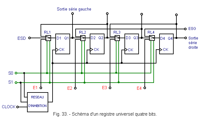
Each of the logical networks RL1, RL2, RL3 and RL4 has the role of guiding one of the three inputs that are applied to the input D of the flip-flop with which it is associated.
This «switching» is performed by the two inputs S0 and S1.
Let's examine each of the modes of operation of the register.
![]() If
S0 = S1 = 0,
the clock signal applied to the CLOCK
input has no action. The outputs of the register remain on their state.
If
S0 = S1 = 0,
the clock signal applied to the CLOCK
input has no action. The outputs of the register remain on their state.
![]() If S0 = 0
and
S1 = 1, then
D4 = ESG ; D3 = Q4 ; D2 = Q3 ; D1 = Q2.
If S0 = 0
and
S1 = 1, then
D4 = ESG ; D3 = Q4 ; D2 = Q3 ; D1 = Q2.
The register is thus «wired» to perform the shift to the left.
The information to be shifted is applied to the left serial input (ESG). The serial output is on output Q1 who which is the left serial output.
![]() If S0 = 1
and S1
= 0, then D1 = ESD ; D2 = Q1 ; D3 = Q2
and D4 = Q3.
If S0 = 1
and S1
= 0, then D1 = ESD ; D2 = Q1 ; D3 = Q2
and D4 = Q3.
The register is thus «wired» to perform the shift to the right.
The information to be shifted is applied to the right serial input (ESD). The serial output is on the Q4 output which is the right serial output.
![]() If S0 = 1
and S1
= 1, then D1 = E1 ; D2 = E2 ; D3 = E3 ; D4
= E4.
If S0 = 1
and S1
= 1, then D1 = E1 ; D2 = E2 ; D3 = E3 ; D4
= E4.
The register is thus «wired» to perform the parallel loading.
The information to be loaded is presented on the parallel inputs E1, E2, E3 and E4. They are stored at each active clock edge on the outputs Q1, Q2, Q3 and Q4 of the register.
We see that the whole operation of a universal register is based on the operation of logical networks RL1, RL2, RL3 and RL4. It is therefore necessary to provide additional information on these.
6. 2. 2. - REVIEW OF A LOGIC NETWORK
The four referral networks of the examined register are identical. Let's analyze the first, in this case RL1. It must match the truth table in Figure 34.
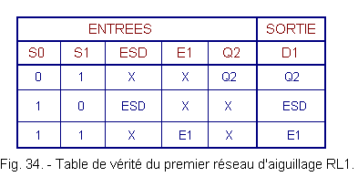
The first line of this table indicates that for S0 = 0 and S1 = 1, the input D1 copies the output Q2 : it is the shift mode on the left.
The second line indicates that for S0 = 1 and S1 = 0, the D1 input copies the ESD input : this is the right shift mode.
The third line indicates that for S0 = 1 and S1 = 1, the input D1 copies the input E1 : it is the LOAD mode.
From this table, we can directly extract the equation of D1 :
D1 = ![]() 0
. S1 . Q2 + S0 .
0
. S1 . Q2 + S0 . ![]() 1
. ESD + S0 . S1 . E1
1
. ESD + S0 . S1 . E1
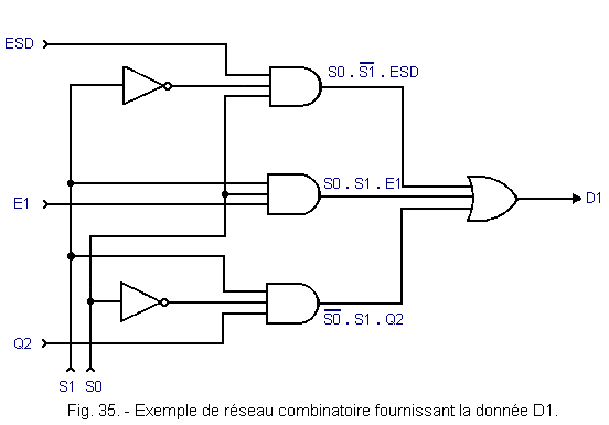
This equation leads us to the combinational network of Figure 35 providing the data D1.
6. 2. 3. - REVIEW OF THE INHIBITION NETWORK
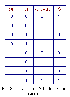
It remains to examine the inhibition network which, from the inputs S0, S1 and CLOCK, generates the clock signal of the four flip-flops.
For the combination S0 = S1 = 0, the CLOCK input must be inactive, ie it must not have any active level transitions on the four clock inputs.
For example, block the output S of this network in logical state 1 when this combination of S0 and S1 occurs.
For the other combinations of S0 and S1, the output S of the muting network must «copy» the CLOCK input.
All of this is reflected in the truth table of Figure 36.
We are taken to the Karnaugh Table in Figure 37.
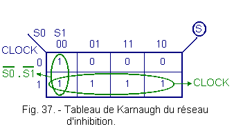
The two groupings of Karnaugh's table give us the following S equation :
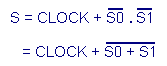
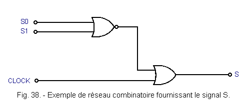
The circuit of Figure 38 can provide the signal S :
The fact that the clock signal comes from a combinatorial network has a disadvantage.
In fact, if one changes S0 or S1 when the CLOCK input is in state 0, a logic level transition can occur at the output S. This can thus cause an active clock edge on the inputs. flip-flops while the CLOCK input has been inactive. Let's take an example where this case occurs.
Suppose that S0 = 0, S1 = 1 and CLOCK = 0, so S = 0 and bring the input S1 to state 0. As a result, since the inputs S0 and S1 are in state 0, the output S Network goes to state 1.
In summary, the input CLOCK remained inactive, when S1 went from state 1 to state 0, the output S went from state 0 to state 1.
We thus obtain an active edge on the clock inputs of the four flip-flops, while the CLOCK input has remained in the 0 state.
To avoid this, inputs S0 and S1 must change state only when the CLOCK input is in state 1.
Thus, the output is forced to state 1, regardless of the variations of S0 and S1.
![]() 6. 2. 4. - ANALYSIS
OF AN UNIVERSAL INTEGRATED REGISTRY : THE 74 194
6. 2. 4. - ANALYSIS
OF AN UNIVERSAL INTEGRATED REGISTRY : THE 74 194
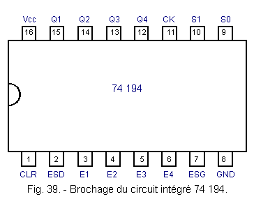
The integrated circuit 74 194 is a 4-bit bidirectional shift register having two control inputs (S0 and S1), a clock input (CK), a serial data input for the left shift (ESG), an input of serial data for the right shift (ESD), four parallel inputs (E1 to E4), one asynchronous general priority reset (CLR) input and four parallel outputs (Q1 to Q4).
The pinout of this circuit is given in Figure 39, while Figure 40 gives its truth table.
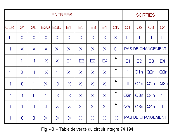
For the second line of the truth table of the integrated circuit 74 194, there is no change in the state of the outputs when CLOCK is in state 0 provided that the inputs S0 and S1 do not change state.
![]() 7. - DYNAMIC REGISTER
7. - DYNAMIC REGISTER
The registers seen so far are of static type because the information stored there can be kept indefinitely provided that the power supply is not disconnected.
This is very convenient because we can read at any time the information that has been loaded, but there is a disadvantage from the integration point of view.
Indeed, each stored binary data requires an entire rocker.
As a result, the integration of high capacity static registers (more than 1000 stages) is limited.
Beyond that, we use dynamic type shift circuits.
They can not memorize the information indefinitely and must therefore scroll them. This characteristic stems from the fact that each memory element is no longer a conventional type of flip-flop, but a circuit that stores the information thanks to the parasitic capacitances of the MOS transistors.
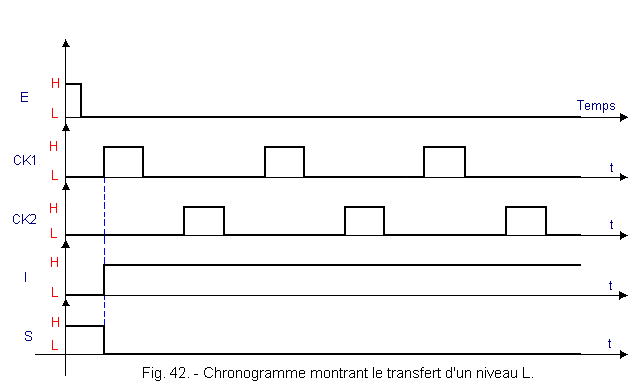
Figure 41 shows the diagram of a dynamic register stage. Each floor like this can store logical data.
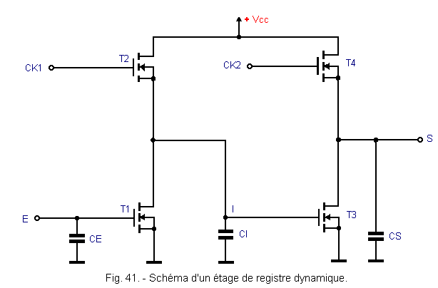
The CE, CI and CS capabilities of Figure 41 are said to be parasitic because they are usually undesirable. They correspond to the gate capacitance of the MOS transistors.
Normally, these should be as small as possible because they disturb the normal operation of the circuit (increase in the propagation time).
In our case, however, they are used to store the information as stored loads.
These capabilities can be loaded or unloaded. A loaded capacity corresponds to a positive information (logical state 1) and a capacity discharged to a negative information (logical state 0).
Suppose that the entry E is subject to the low level (L). The transistor T1 is blocked.
When the clock input CK1 goes to the level H, the transistor T2 is turned on and thus charges the capacity CI at + Vcc.
Therefore, the transistor T3 is conductive and it discharges the capacitor CS, if it was loaded.
Output S goes to the L level and we can say that the L level present at the E input has been transferred to the S output. This is shown in Figure 42.
When a positive pulse occurs on the clock input CK2, the transistors T3 and T4 are simultaneously conducting.
On the other hand, from the technological point of view, these two transistors are different and their respective saturation resistance is such that the potential of the point S is much closer to zero than of the voltage + Vcc : the output S therefore remains at the logic level L.
If now the input E is subjected to the level H, the transistor T1 begins to drive. The capacitance CI is discharged and the point I is brought to the level L as shown in the chronogram of Figure 43.
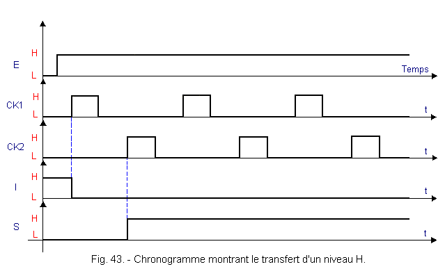
When a positive pulse occurs on the clock input CK1, the two transistors T2 and T1 are saturated simultaneously and as they are made technologically in the same way as the pair T4-T3, the point I is maintained at logic L despite the conduction of T2.
At the next clock pulse on CK2, transistor T4 starts driving and loads the capacitor CS at level H.
The output S thus goes to the level H and the level H present at the input E has been transferred to the output S.
In summary, in a dynamic register stage (here two clock phases), a data applied to the input is found at the output when two pulses CK1 and CK2 are applied.
It is however necessary that the signals CK1 and CK2 are at a sufficient frequency (about 10 kHz) so that the parasitic capacitances of the MOS transistors do not have time to load or discharge between two successive pulses.
The next
theory will deal with counters and frequency dividers.
 Click here for the next lesson or in the summary provided for this purpose. Click here for the next lesson or in the summary provided for this purpose. |
 Top of page Top of page |
|
Previous Page |
 Next Page Next Page |
Nombre de pages vues, à partir de cette date : le 27 Décembre 2019

Envoyez un courrier électronique à Administrateur Web Société pour toute question ou remarque concernant ce site Web.
Version du site : 10. 4. 12 - Site optimisation 1280 x 1024 pixels - Faculté de Nanterre - Dernière modification : 02 Septembre 2016.
Ce site Web a été Créé le, 14 Mars 1999 et ayant Rénové, en Septembre 2016.