 Serial input register and serial output
How does a Shift Register Work ? :
In this theory, we will examine the shift circuits also called shift registers.
These circuits are most often formed of synchronous flip-flops connected one after the other and controlled by the same clock signal.
The state of the first flip-flop shifts to the following flip-flops, hence the name of «shift circuits».
They are widely used as timing circuit, memory circuit and information processing.
An important application of shift registers is the serial transmission of logical data.
We will see that the shift registers can take different forms according to access to inputs and outputs.
![]() 1. - INPUT
REGISTER SERIES AND OUTPUT SERIES
1. - INPUT
REGISTER SERIES AND OUTPUT SERIES
1. 1. - HOW DOES A SHIFT REGISTER WORK ?
To understand the operation of the shift registers, in particular the serial input and serial output register, we will take into consideration the very simple circuit of Figure 1.
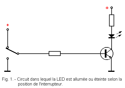
We deduce, by observing this figure, that the LED lights up if the switch is switched upward, which causes the transistor to drive.
On the other hand, the LED is off if the switch is switched down which blocks the transistor.
Thus, the LED faithfully and immediately follows the commands from the switch; each opening or closing of it produces an instantaneous effect on the state of the LED.
In other words, the information on the state of the switch is transmitted immediately (apart from the switching time of the transistor).
Let us now observe the circuit of figure 2. A synchronous rocker of type D is interposed between the switch and the LED.
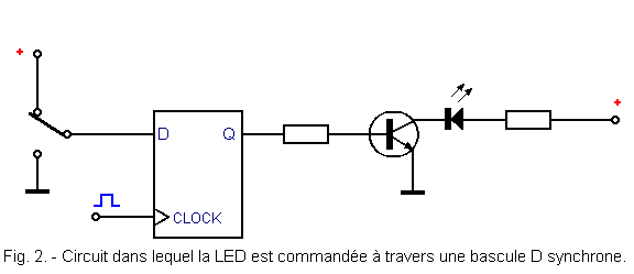
In this case, the status information of the switch is not transmitted immediately to the LED, as it is necessary to apply a pulse on the CLOCK input.
The Q output of the flip-flop goes into the state determined by the position of the switch each time a pulse is applied to the CLOCK input.
We are informed about the state of the switch with a certain delay.
Let's change the circuit now by changing the number of flip-flops to four as shown in Figure 3.
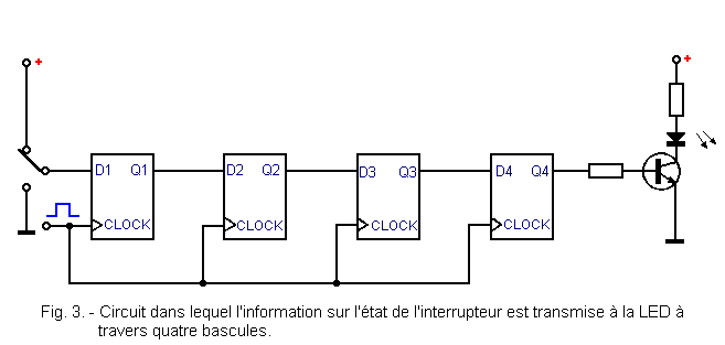
In this new circuit, the flip-flops are connected in cascade ; the output of one is connected to the input of the next.
The CLOCK inputs, on the other hand, are all interconnected. Thus, a single clock input controls the four flip-flops simultaneously.
Since four flip-flops are interposed between the switch and the LED, four clock pulses are required to transmit the status information of the input switch to the output of the circuit where the LED is located.
The first pulse transfers information from the input to the output of the first flip-flop, the second transmits it to the output of the second flip-flop and so on until the fourth.
The information is shifted by propagating from the input of the first flip-flop to the output of the fourth flip-flop after four clock pulses.
The circuit of Figure 3 constitutes a shift register.
![]() 1. 2. - REGISTER WITH SHIFT USED AS TIMING CIRCUIT
1. 2. - REGISTER WITH SHIFT USED AS TIMING CIRCUIT
We will see now what can serve this type of circuit which, apparently, only complicates the transmission of the control of the switch.
An application of the shift register is to use it as a timing circuit.
Let's take the circuit of Figure 3 and suppose that the outputs of the four flip-flops are at the low level and that we switch the switch to the positive voltage.
We note from Figure 4 that between the time t0 when we close the switch (position «+») and the time t4 where the LED is lit, three periods of clock flow . The interval t0 to t4 is the time taken by the state of the switch to reach the output of the assembly where it determines the lighting of the LED.
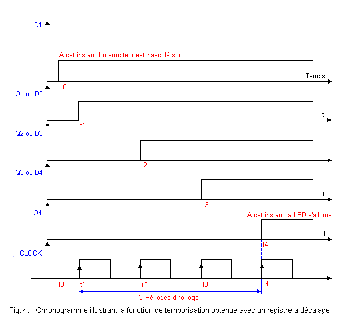
If we connect the LED indicator circuit to the output of the third flip-flop, the delay obtained is two periods and one clock period if it is connected to the output of the second flip-flop.
We can also play on the frequency of the clock pulses to vary the delay.
In summary, by playing on the number of flip-flops and on the frequency of the clock signal, it is possible to obtain a delay of any duration.
1. 3. - SHIFT REGISTER USED AS DELAY CIRCUIT
In the example we have just examined, the switch is switched to the positive voltage at the beginning of the experiment and remains in this position until the end thereof.
After four clock pulses, the output goes to level H.
But nothing prohibits switching the switch between a clock pulse and the next.
In this case, the output of the circuit faithfully follows these switches, but with a delay of three clock periods corresponding to four active transitions of the clock signal.
Figure 5 shows the timing of the signals D1, Q4 and CLOCK as a function of time.
.gif)
It is clear that the information present in D1 is found in Q4 after four clock pulses.
The examined register is the simplest of the shift circuits.
It is called shift register with serial input and serial output or more simply serial-serial register.
This name comes from the fact that the information relating to the state of the switch, are presented at the input of the circuit sequentially one after the other, that is to say in series. Input D1 is the serial input of the register.
In the same way, they present themselves at the exit one after the other, so in series. Output Q4 is the serial output of the register.
![]() 2. - INPUT REGISTER WITH SERIES AND
PARALLEL OUTPUTS
2. - INPUT REGISTER WITH SERIES AND
PARALLEL OUTPUTS
2. 1. - OPERATION
If we delete the LED indicator circuit and the input switch of the circuit of Figure 3, there remains only the series-serial shift register itself which we have seen two applications.
We will now analyze a third, in which the shift register is used as delay and phase shift circuit of a rectangular signal.
For this, it is necessary to modify the circuit as shown in Figure 6, that is to say add three other intermediate outputs corresponding to the outputs of each flip-flop.
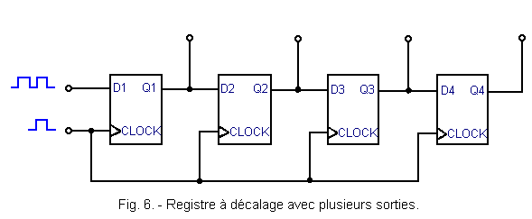
We apply to the input D1 of the circuit a rectangular signal of lower frequency than the clock signal applied to the CLOCK input.
At the outputs Q1, Q2, Q3 and Q4 of the register appear four signals identical to each other but delayed, that is to say out of phase with each other by a time equal to the period of the clock signal. (Figure 7).
The explanation of the timing diagram of Figure 7 is simple :
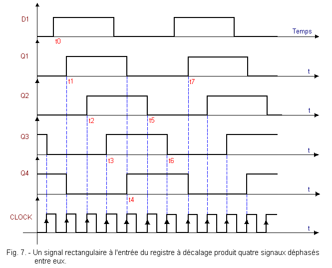
The rectangular signal at the input of the circuit propagates from one flip-flop to the other by shifting from one position to each clock pulse.
These out-of-phase signals can be used to produce repetitive commands. We thus obtain a sequence of signals which can be used to make an automatism of which we will analyze a simple and concrete example.
2. 2. - APPLICATION TO THE SEQUENTIAL CONTROL OF LAMPS
If, as in the example shown in Figure 8, we connect four lamps to the four outputs of the register, the lamps will light sequentially.
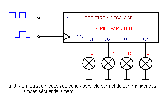
Indeed at time t1 (Figure 7), the output Q1 goes to level H and therefore the lamp L1 lights while the other lamps remain off.
At time t2, the output Q2 goes to the level H and the lamp L2 turns on (L1 remains lit).
At time t3, the output Q3 goes to level H and L3 turns on (L1 and L2 also on).
At time t4, two changes occur : the output Q4 goes to the H level and L4 turns on, but at the same time, the output Q1 goes back to the level L and thus the lamp L1 goes out.
At time t5, L2 turns off
At time t6, L3 goes out.
The cycle described from time t1 to time t6 continues indefinitely.
We can imagine more complicated cycles by increasing the number of flip-flops in the register.
For example, instead of lamps, we can assume that there are commands from a machine tool in order to automate it.
The register that we have just examined is a register with serial input and parallel outputs or more simply a serial-parallel register.
We will now analyze an integrated registry of this type.
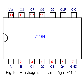
2. 3. - ANALYSIS OF AN INTEGRATED SERIES - PARALLEL REGISTER : 74164
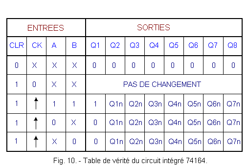
Integrated circuit 74164 is a two-input and eight-output parallel shift register having a clock input (CK) and an asynchronous general priority reset (CLR) input.
The pinout of this circuit is given in Figure 9, while Figure 10 gives its truth table.
NOTE :
The appellations Q1n, Q2n, Q3n, etc ... that appear in the truth table of the integrated circuit 74164 are probably unknown to you. These designations simply mean that the output considered has the state that the previous latch had before the clock stroke. For example, in the 3rd row of the table (when A and B are at 1), we read in Q2 the state Q1n, which means that Q2 is in the state where Q1 was before the clock which raised Q1 to 1.
![]() 3. - REGISTER WITH PARALLEL INPUTS AND
SERIAL OUTPUT
3. - REGISTER WITH PARALLEL INPUTS AND
SERIAL OUTPUT
Serial-parallel or serial-series registers are used to shift information to the right by applying them one by one on the serial input.
This means that the data is available in series, or on a single wire. But there may be the case where several data are available simultaneously.
It is therefore necessary to be able to enter these data at the same time in the register ; this is achieved by means of several so-called parallel inputs.
The operation which consists in positioning each latch of the register with the level present on the corresponding parallel input is called the loading (LOAD in English) of the register. This loading can be done asynchronously or synchronously using a command entry called SHIFT / LOAD.
If the load is asynchronous, as soon as the SHIFT / LOAD input is activated, each output of the register copies the current state to its parallel input.
If, on the other hand, the loading is synchronous, it is also necessary to apply a clock pulse so that each latch of the register stores the previous state on its parallel input.
If the SHIFT / LOAD input is not enabled, the register operates in serial-serial mode.
3. 1. PARALLEL REGISTER - ASYNCHRONOUS LOADING SERIES
Figure 11 represents a 4-bit parallel-serial register (because it has 4 stages) whose loading is done asynchronously.
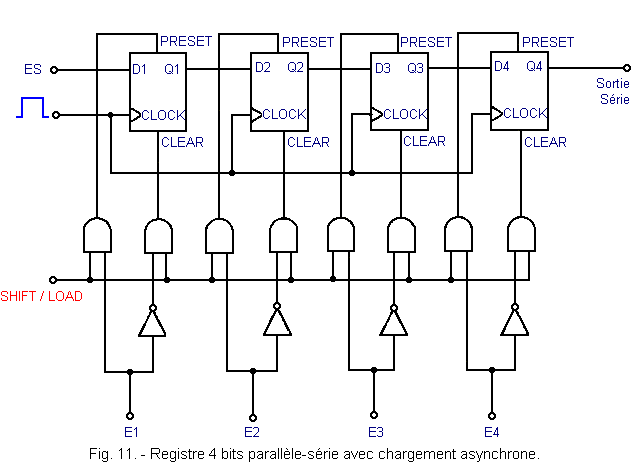
Compared to the previous registers, there appears a combinatorial network of logic gates. These act on the CLEAR and PRESET asynchronous inputs of each flip-flop.
The loading of the register, which consists in positioning the outputs Q1, Q2, Q3 and Q4 with the logic levels present on the parallel inputs E1, E2, E3 and E4, will therefore be asynchronous.
The two modes of operation, shift and load, are differentiated by the SHIFT / LOAD command input.
Depending on the level applied to this input, the register operates in SHIFT mode, that is to say in offset mode or in LOAD mode, that is to say in loading mode.
3. 1. 1. - LOAD MODE EXAMINATION
To proceed with the loading (parallel) of the register, it is necessary to apply a level H to the entry SHIFT / LOAD.
Indeed, the AND gates of the network are validated and the inputs E1, E2, E3 and E4 thus act on the CLEAR and PRESET inputs of each flip-flop.
To understand how to perform the asynchronous loading of the register, consider the action of the input E1 on the first flip-flop.
Since the SHIFT / LOAD input is raised to the H level, the logical level applied at E1 is found on the PRESET input of the flip-flop, while the CLEAR input receives the logical level opposite to that of E1.
Since the CLEAR and PRESET inputs are active at the H level, when E1 is at the H level, the PRESET input becomes active and the Q1 output of the flip-flop thus goes to the H level.
If on the other hand, the input E1 is at the level L, it is the entry CLEAR which becomes active and thus the rocker is carried to the level L.
In summary, when the SHIFT / LOAD input is at the H level, the output Q1 «copies» the input E1.
The same goes for the other outputs Q2, Q3 and Q4 which respectively copy the inputs E2, E3 and E4.
As long as we are in the loading phase, the clock signal has no influence since one of the two inputs CLEAR or PRESET is active, therefore a priority.
3. 1. 2. - EXAMINING THE SHIFT MODE
Let's now return the SHIFT / LOAD entry at the L level. Therefore, the CLEAR and PRESET entries become inactive since they go to the L level regardless of the level of the parallel inputs.
The clock signal becomes dominant and the register operates in SHIFT mode.
At each clock pulse, the data present in D1 is transferred to Q1, that present in Q1 is transferred to Q2 and so on until the output Q4.
It should be noted that the data present in Q4 is lost at each clock pulse.
The data on E1, E2, E3 and E4 may vary, they have no influence on the shift mode operation of the register.
In summary, the 4-bit information on the parallel inputs is loaded on a high level of the SHIFT / LOAD input. By returning this input to the level L, the loaded information shifts to the right one notch at each clock pulse.
We will now analyze an integrated registry of this type.
3. 1. 3. - ANALYSIS OF A PARALLEL REGISTER - INTEGRATED ASYNCHRONOUS SERIES : THE 74165
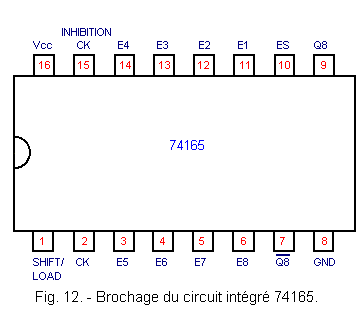
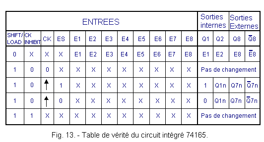
The integrated circuit 74165 is an 8-bit shift register with a serial input (ES) and an output (Q8). It has eight parallel inputs (E1 to E8), an asynchronous shift and load control input (SHIFT / LOAD), a clock input (CK) and an inhibit input (CK INHIBIT). It should be noted that these two inputs CK and CK INHIBIT are interchangeable.
The pinout of this integrated circuit is given in Figure 12, while Figure 13 gives its truth table.
![]() 3. 2. - PARALLEL REGISTER - SYNCHRONOUS LOAD SERIES
3. 2. - PARALLEL REGISTER - SYNCHRONOUS LOAD SERIES
The previous registry allowed to pre-position its content asynchronously.
We will now see how to load the register synchronously.
To obtain this result, it suffices to replace the combinational network of Figure 11 by another network acting either on the asynchronous inputs CLEAR and PRESET, but on the synchronous inputs D1, D2, D3 and D4 of the flip-flops.
Each latch-specific part of the latch includes a control input corresponding to the SHIFT / LOAD input, two data inputs, and one output.
Figure 14 shows how is structured the parallel-serial register with synchronous loading.
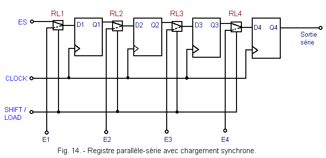
Each of the parts of the combinational network, identified by the symbols RL1, RL2, RL3 and RL4 in Figure 14, can be likened to a logical data switching.
Depending on the level of the control input, the circuit will «point» either of the two inputs to the output. In other words, the output will «copy» one of the two inputs.
Let us analyze, for example, the first combinational network RL1 of the assembly of Figure 14, the three others being strictly identical to the first.
Suppose that when the SHIFT / LOAD entry is at 0, D1 = ES and D1 = E1 when the SHIFT / LOAD entry is at 1 (the inverse may exist).
The truth table in Figure 15 illustrates the operation of the RL1 network.
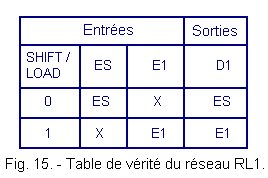
The first line of this table indicates for SHIFT / LOAD = 0, the output D1 copies the input ES regardless of the state of E1.
The second line indicates that for SHIFT / LOAD = 1, the output D1 copies the input E1 regardless of the state of ES.
These two lines make it possible to find the following equation of D1 :
![]()
This equation can also be written as :
![]()
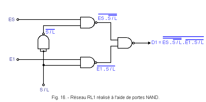
This new form of the equation of D1 allows us to simplify it according to DE MORGAN's theorem in order to realize the RL1 network using NAND gates. We obtain as follows :
![]()
We thus come to the diagram of Figure 16.
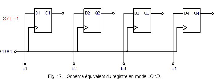
3. 2. 1. - LOAD MODE EXAMINATION
If the SHIFT / LOAD input is in state 1, the output of each network is at the same logic level as the corresponding parallel input.
In other words, D1 = E1, D2 = E2, D3 = E3 and D4 = E4.
We can say that the four inputs E1, E2, E3 and E4 are respectively directed to the inputs D1, D2, D3 and D4 flip-flops.
The register is then ready to be loaded with the levels present on the parallel inputs.
Just send a clock pulse to the CLOCK input so that Q1 = E1, Q2 = E2, Q3 = E3 and Q4 = E4.
The loading of the register is thus synchronous.
We obtain the equivalent diagram of Figure 17.
3. 2. 2. - EXAMINING THE SHIFT MODE
If the SHIFT / LOAD input is in the 0 state, the register operates in SHIFT or offset mode.
Indeed, the input ES is connected through the first network to the input D1 of the first flip-flop.
Similarly, the outputs Q1, Q2 and Q3 are «connected» respectively to the inputs D2, D3 and D4 through the second, third and fourth networks.
We can say that D1 = ES, D2 = Q1, D3 = Q2 and D4 = Q3.
Figure 18 shows the equivalent scheme of the register in SHIFT mode.

At each clock pulse, the contents of the register are shifted one step to the right.
The data present in ES is stored in Q1, while the data present in Q4 is lost.
By combining the two modes of operation of the register, we can, initially, load it with information, then in a second time, shift it one or more steps to the right.
We will now analyze an integrated registry of this type.
3. 2. 3. - ANALYSIS OF A PARALLEL REGISTER - INTEGRATED SYNCHRONOUS SERIES : 74166
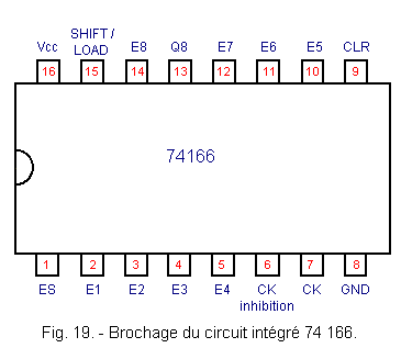
Integrated circuit 74166 is an 8-bit serial input (ES) shift register and a serial output (Q8). It has eight parallel inputs (E1 to E8), a general priority reset asynchronous input (CLR), a synchronous shift and load control input (SHIFT / LOAD), a clock input (CK) and an input inhibit clock (CK INHIBIT), these two inputs being interchangeable.
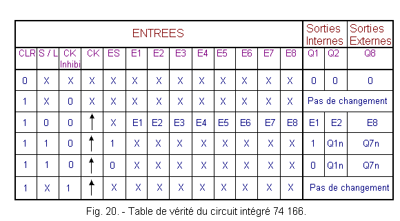
The pinout of this circuit is given in Figure 19, while Figure 20 gives its truth table.
NOTE :
Contrary to the example chosen for our theoretical explanations, it should be noted that the integrated circuit 74166 is in LOAD mode when its control input SHIFT / LOAD is in state 0, and in SHIFT mode when this same input is at the same time state 1.
 Click here for the next lesson or in the summary provided for this purpose. Click here for the next lesson or in the summary provided for this purpose. |
 Top of page Top of page |
|
Previous Page |
 Next Page Next Page |
Nombre de pages vues, à partir de cette date : le 27 Décembre 2019

Envoyez un courrier électronique à Administrateur Web Société pour toute question ou remarque concernant ce site Web.
Version du site : 10. 4. 12 - Site optimisation 1280 x 1024 pixels - Faculté de Nanterre - Dernière modification : 02 Septembre 2016.
Ce site Web a été Créé le, 14 Mars 1999 et ayant Rénové, en Septembre 2016.