 Different types of JK flip-flops
Toggle JK Master Slave :
3. - JK MASTER SLAVE ROCKET
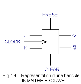
3. 1. - SYMBOLIC REPRESENTATION The rocker JK MASTER SLAVE is another rocker of type MASTER SLAVE. As shown in Figure 29, the flip-flop JK has two entries denoted J and K while the flip-flop D MASTER SLAVE has only one.
We find the CLOCK clock entry, CLEAR and PRESET reset and reset entries, and the complementary Q and 3. 2. - STRUCTURE AND PRINCIPLE OF OPERATION
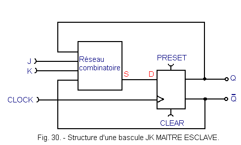
The rocker JK MASTER SLAVE is elaborated from a rocker D MASTER SLAVE. It suffices to add a combinational network on the input D (see Figure 30) to obtain the JK flip-flop.
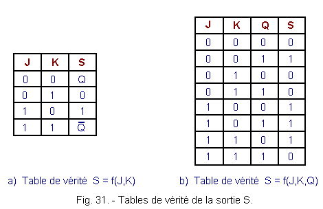
Depending on the state of the inputs J and K, the output S of the combinational network connected to the input D of the flip-flop D MASTER SLAVE has one of the four states shown in Figure 31-a. We are led to the truth table of Figure 31-b which gives the logical state of S according to the possible combinations of the logical states of the inputs J, K and Q.
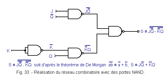
Let's draw Karnaugh's picture (Figure 32) to find the simplest equation of S. The two groupings in this table are used to find the following logical equation for S : S = J By using NAND gates, the following combinational circuit (Figure 33) can provide the signal S :
![]() outputs of the D MASTER SLAVE..
outputs of the D MASTER SLAVE..
.gif)
![]() +
+ ![]() Q
Q
3. 3. - EXAMINATION
OF THE FOUR OPERATING MODES FROM THE TABLE OF TRUTH IN THE FIGURE 31-a
If J = 0 and K = 0, then S = D = Q. This means that the logical state present in D is the same as that of the output Q. There can therefore be no tilting at the moment of the active edge of the clock and the output status Q and If J = 0 and K = 1, then S = D = 0. The logical state that the JK latch stores during the active edge of the clock is the logic state 0. It is the resetting of the flip-flop which is therefore synchronous as opposed to the CLEAR entry which is priority and asynchronous. If J = 1 and K = 0, then S = D = 1. The logical state stored by the JK flip-flop during the active edge of the clock is logic state 1. This is the resetting of the flip-flop which is also synchronous. If J = 1 and K
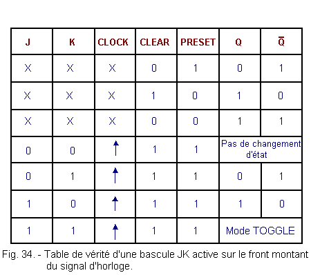
= 1, then S = D = So at each active edge of the clock, the output Q switches to take the state of 3. 4. - TABLE OF TRUTH AND CHRONOGRAM The complete operation of the JK MASTER SLAVE rocker is summarized by the truth table in Figure 34. The first three rows of this table indicate that the CLEAR and PRESET entries are priority and active on a low level. The following four lines correspond to the four modes of operation discussed previously. To illustrate this truth table, consider the timing chart in Figure 35.
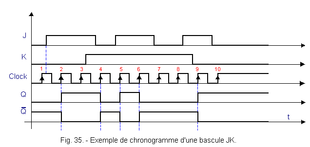
Note in this figure that each rising edge of the CLOCK input is assigned an upward arrow. This indicates that the examined JK flip-flop switches on the rising edge. It is assumed that the entries CLEAR and PRESET are inactive because the logical state 1 is permanently applied to them.
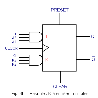
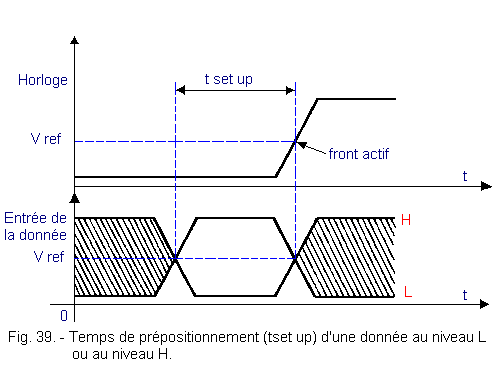
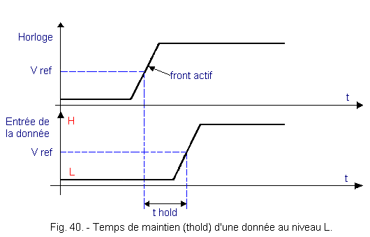
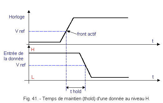
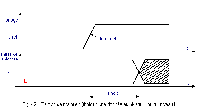
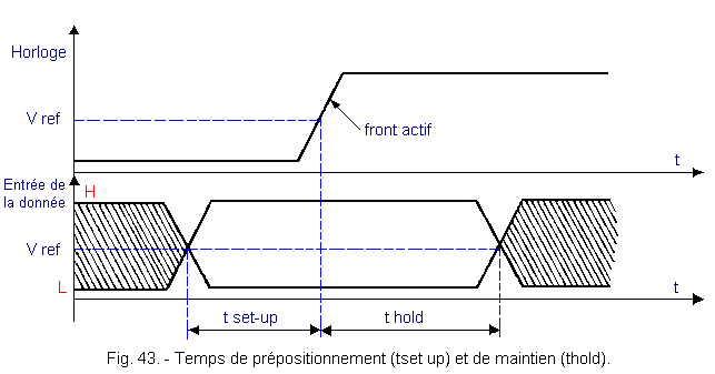
Just before the first active front of the clock, the inputs J and K are at 0. So at this front, the flip-flop does not switch and the output Q remains in the state where it is, that is to say say here the state 0. Before the second rising edge of the clock is applied, the input J goes to state 1. The output Q thus goes to state 1. At the third active edge of the clock, J = 1 and K = 0. The latch that was in state 1 remains in this state. At the fourth active edge of the clock, J = 0 and K = 1. The toggle switches to state 0. At the fifth active edge of the clock, J = 1 and K = 1. The toggle switch therefore switches to the complementary state of the previous state, the state 1. This is the TOGGLE mode. At the sixth active edge of the clock, J = 1 and K = 1. The toggle switches back to state 0 (TOGGLE). At the seventh active edge of the clock, J = 0 and K = 1. The flip-flop that was in state 0 remains in this state. At the eighth active edge of the clock, J = 0 and K = 1. The flip-flop remains in state 0. At the ninth active edge of the clock, J = 1 and K = 0. The flip-flop thus goes to state 1. At the tenth active edge of the clock, J = 0 and K = 0. The toggle does not change state and therefore remains in state 1. This is the memory position. Unlike the JK flip-flop described above, a majority of JK flip-flops are sensitive to the falling edges ( There are also flip-flops JK MASTER SLAVE whose data transfer takes place in two stages. On the rising edge of the clock, the data is stored in the MASTER, and this is transferred to the output of the SLAVE on the falling edge. In the truth tables of these latches, this operating mode is indicated in the column assigned to the CLOCK input by the symbol P. As in the case of flip-flop D, the PRESET and CLEAR inputs can be active in state 0 or in state 1 according to the internal constitution of the flip-flop. There are also JK flip-flops with multiple inputs. Figure 36 shows one having six entries denoted J1, J2, J3, K1, K2, K3. The operation of such a flip-flop is similar to that of a conventional JK flip-flop. Just replace J and K with : J = J1 . J2 . J3 K = K1 . K2 . K3 This type of scale was used to make counters. Since these are available as integrated circuits, multiple-input JK flip-flops are no longer used. The manufacturer defines a certain number of dynamic parameters that must be respected in order to obtain a correct operation of the circuit used. 4. 1. - TIME TO SET UP TIME IN A DATA ON A DEPENDENT INPUT OF THE CLOCK The prepositioning time is the minimum time during which the data present on the input must remain stable before the active edge of the clock signal for it to be recognized. If this time is not respected, the data will not be taken into account by the circuit. Figure 37 illustrates the preset time (tset up) when the data to be memorized is at the level L. V ref corresponds to the tilting voltage of the circuit gates : Figure 38 illustrates the prepositioning time when the data to be memorized is at level H. The two chronograms of Figures 37 and 38 are often combined into one in the manufacturer's catalogs, as shown in Figure 39. The hatched periods indicate that the data may vary from one level to another without any influence on the behavior of the circuit. 4. 2. - HOLD TIME IN ENGLISH OF A DATA ON A DEPENDENT INPUT OF THE CLOCK The hold time is the minimum time during which the data present on the input must remain stable after the active edge of the clock for this data to be recognized. Figure 40 illustrates the hold time (thold) when the data to be memorized is at the level L. Figure 41 illustrates the hold time when the data to be memorized is at level H. The two chronograms of Figures. 40 and 41 can, in the same way as above, be combined into one, as shown in Figure 42. In the manufacturer's catalogs, the two timing diagrams that represent the prepositioning and holding times are grouped into one, as shown in Figure 43.
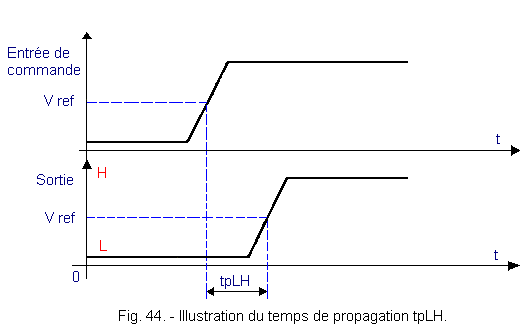
4. 3. - TIME OF PROPAGATION OF AN ENTRY TO AN OUTPUT 4. 3. 1. - TIME OF PROPAGATION
"tpLH" The propagation time tpLH
is the time that elapses between the moment when the control input becomes active and the moment when the output goes from L to H. The control input can be the clock input, the CLEAR input, or the PRESET input. This time noted tpLH
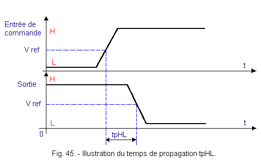
is specified for a given input (CLOCK, CLEAR or PRESET) and a given output (Q or In practice, this time corresponds to the delay brought by the internal doors of the circuit. Figure 44 illustrates the time tpLH. 4. 3. 2. - TIME OF PROPAGATION tpHL The propagation time tpHL
is the time that elapses between the moment when the control input becomes active and the moment when the output goes from level H to level L. Figure 45 illustrates this time
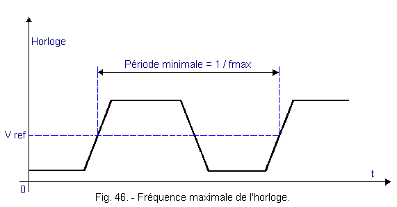
tpHL. 4. 4. - MAXIMUM FREQUENCY OF THE CLOCK This operating limit frequency fmax is due to the delay brought by the doors of the circuit. It corresponds to a minimum period 1 / fmax of the clock signal as shown in Figure 46.
Envoyez un courrier électronique à Administrateur Web Société pour toute question ou remarque concernant ce site Web.
Version du site : 10. 4. 12 - Site optimisation 1280 x 1024 pixels - Faculté de Nanterre - Dernière modification : 02 Septembre 2016.
Ce site Web a été Créé le, 14 Mars 1999 et ayant Rénové, en Septembre 2016.
![]() remain unchanged.
remain unchanged.![]() .
The logical state which is memorized at the output Q during the active edge of the clock is that of the output
.
The logical state which is memorized at the output Q during the active edge of the clock is that of the output ![]() .
.![]() and vice versa. This mode of operation already seen with the flip-flop D MASTER SLAVE is the TOGGLE mode. It is the frequency divider by 2, the outputs Q and
and vice versa. This mode of operation already seen with the flip-flop D MASTER SLAVE is the TOGGLE mode. It is the frequency divider by 2, the outputs Q and
![]() are at a frequency 2 times smaller than the frequency of the clock signal.
are at a frequency 2 times smaller than the frequency of the clock signal.
![]() 3. 5. - DIFFERENT
TYPES OF JK ROCKETS
3. 5. - DIFFERENT
TYPES OF JK ROCKETS
![]() )
of the clock signal and not to the rising edges (
)
of the clock signal and not to the rising edges (![]() ).
).
![]() 4. - DYNAMIC PARAMETERS OF A SYNCHRONOUS ROCKER
4. - DYNAMIC PARAMETERS OF A SYNCHRONOUS ROCKER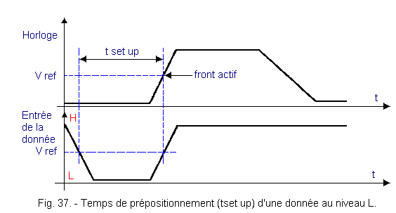
![]() V ref = 1,5 V in tandard TTL technology.
V ref = 1,5 V in tandard TTL technology.![]() V ref = 1,3 V in TTL - LS technology.
V ref = 1,3 V in TTL - LS technology.![]() V ref = VDD / 2 in C.MOS technology, VDD being the supply voltage of the circuit.
V ref = VDD / 2 in C.MOS technology, VDD being the supply voltage of the circuit.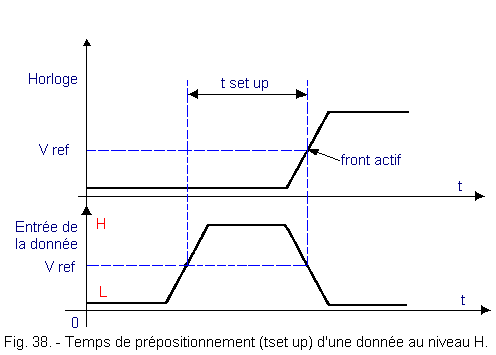
![]() ).
).
 Click here for the next lesson or in the summary provided for this purpose.
 Top of page
Previous Page
 Next Page
Nombre de pages vues, à partir de cette date : le 27 Décembre 2019
