 Multivibrators with Transistors Multivibrators with Transistors |
Bistable flip-flop realized with NAND doors
|
Multivibrators R.S.C. |
|
Multivibrators of type «D» or «LATCH»
|
Footer |
Bistables Multivibrators - Transistors Multivibrators - R.S.C. Multivibrators - Type D Multivibrators :
3. - THE MULTIVIBRATORS BISTABLES
3. 1. - DIFFERENT TYPES OF BISTABLE MULTIVIBRATORS
These are circuits whose outputs have two stable states 1 or 0. They have the property of maintaining these stable states after the disappearance of the logical level or levels that gave rise to these stable states. These circuits are considered as memory elements capable of storing and providing a unit of information, that is, a bit.
The flip-flop R-S or «FLIP-FLOP» is the simplest type of these new circuits. There are two types of «FLIP-FLOP», «FLIP-FLOP R-S» and «FLIP-FLOP Clock».
In this theory, we will consider the asynchronous flip-flops, that is to say the R-S flip-flop and its derivatives, as well as the D flip-flops controlled by a logic level. Clock D flip-flops and J-K flip-flops are synchronous circuits and will be discussed in theory 5.
3. 2. - CROSS COUPLES MULTIVIBRATORS
3. 2. 1. - CROSSED COUPLED MULTIVIBRATOR R-S REALIZED WITH NOR DOORS
a) Operation
This is the rocker examined previously. His diagram is shown in Figure 35.
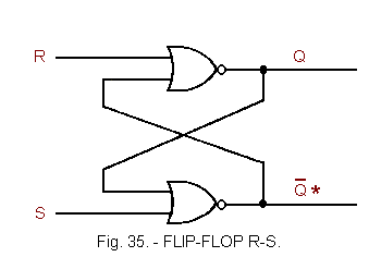
We usually call the outputs of a flip-flop, Q and ![]() ; however, we will adopt the notation
; however, we will adopt the notation ![]() ; Indeed,
; Indeed, ![]() is not always the complement of Q.
is not always the complement of Q.
The rocker is called SET when Q = 1 and ![]() = 0, it is called RESET when Q = 0 and
= 0, it is called RESET when Q = 0 and ![]() = 1.
= 1.
The inputs R (Reset) and S (Set) are active at logic level H.
Let us return to the examination of this scale by showing its operation by means of a table presenting all the successive cases that we can meet.
This table is shown in Figure 36.
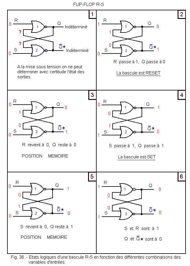
Figure 36 shows the evolution of the circuit from power on.
The states of the inputs are indicated for each case as well as the corresponding states of the outputs.
We see that there exists in this rocker an entry R and an entry S.
In the first case, only the state of one of the two inputs of the NOR gates is known (level L). We can not say what is the state of the outputs, in fact, it depends on the state of the second input NOR.
In the second case, a level H is applied to the input R, which has the effect of forcing the first NOR to 0. This 0 brought back on the upper input of the second NOR forces the output of this one to 1. This output being brought back to the lower input of the first NOR comes to confirm the forcing thereof to 0.
This leads to the first stable state of the rocker (RESET).
In the third case, R has returned to 0, it is found that given the previous state, the rocker is maintained RESET, the first NOR being forced to 0 by its lower input. The output of the second NOR is then maintained at 1 because its two inputs are in state 0. The effect caused by R = 1 has been memorized in the second case.
In the fourth case, S goes to 1 and comes to force the second NOR to 0. By the same process due to the back-coupling of the NOR, we thus end up with the setting of the flip-flop or SET (second stable state).
In the fifth case, S has returned to 0, we note the maintenance of the flip-flop to 1.
In the sixth case, R and S are at 1 simultaneously and the two NOR gates are forced to 0.
b) Truth Table
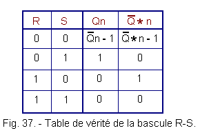
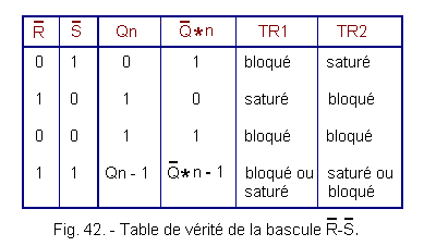
We can summarize this operation in the form of a truth table. We will call Qn the state of the output Q at the instant n and Qn - 1 the state of the output Q at the moment n - 1, that is to say at the moment preceding the change of state of entries.
In a similar way, we will take the notations
![]() n
and
n
and ![]() n - 1.
n - 1.
This truth table is shown in Figure 37.
![]() 3. 2. 2. - MULTIVIBRATORS WITH TRANSISTORS
3. 2. 2. - MULTIVIBRATORS WITH TRANSISTORS
a) Reminders on the transistors
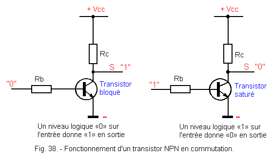
Figure 38 recalls the operation of the switching NPN transistor as you have seen in technology 1. (Digital and fundamental technology summary).
b) The multivibrators ![]() with transistors.
with transistors.
In its simplest form with discrete components, the FLIP-FLOP circuit is constituted as shown in Figure 39.
Let's analyze how this circuit works :
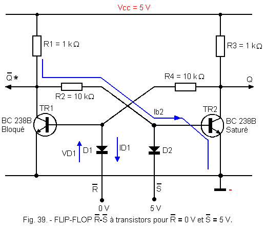
When one applies 0 volt on the entry ![]() (
(![]() is with 5 volts), the diode D1 is crossed by a current ID1 (figure 39) and a very low voltage VD1 appears at its terminals.
is with 5 volts), the diode D1 is crossed by a current ID1 (figure 39) and a very low voltage VD1 appears at its terminals.
The transistor TR1 is then blocked (base insufficiently positive for it to drive). TR1 being blocked, no current flows through it and ![]() rises to about 5 volts.
rises to about 5 volts.
This voltage is then returned through R2 on the basis of TR2 which saturates (current Ib2). Q then drops to practically 0 volt. This voltage brought back through R4 on the basis of TR1 comes to maintain the blocking of it, even if the entry ![]() goes back to 5 volts.
goes back to 5 volts.
We obtain a first stable state : TR1 is blocked, TR2 is saturated. Thus, the ![]() output goes to 5 volts (level H) and the output Q goes to 0 volt (level L). The application of a «0» on the entry
output goes to 5 volts (level H) and the output Q goes to 0 volt (level L). The application of a «0» on the entry ![]() thus entails Q = 0 and
thus entails Q = 0 and ![]() = 1. It is the state RESET of the rocker.
= 1. It is the state RESET of the rocker.
If now the entry ![]() passes to 0 volt and
passes to 0 volt and ![]() is at 5 volts (Figure 40), in the same way TR2 hangs (0 volt on its base) and the output Q goes to 5 volts (level H). The transistor TR1 saturates, so the exit
is at 5 volts (Figure 40), in the same way TR2 hangs (0 volt on its base) and the output Q goes to 5 volts (level H). The transistor TR1 saturates, so the exit ![]() passes to the level L.
passes to the level L.
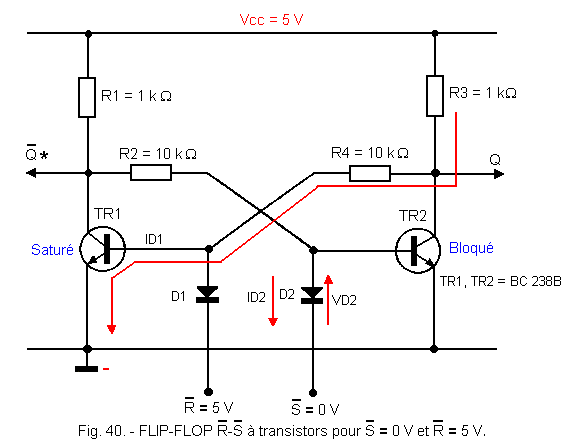
This is the second stable state of the flip-flop. TR2 is blocked and TR1 is saturated.
So ![]() = 0 causes Q = 1 and
= 0 causes Q = 1 and ![]() = 0. This is the SET state of the flip-flop.
= 0. This is the SET state of the flip-flop.
When, as represented in Figure 41, ![]() = 0 V and
= 0 V and ![]() = 0 V, TR1 and TR2 are blocked because their base is maintained at about 0 Volt (Q
=
= 0 V, TR1 and TR2 are blocked because their base is maintained at about 0 Volt (Q
= ![]() = 5 volts is the level «H»).
= 5 volts is the level «H»).
The direction of the currents in the diodes are indicated by the blue and red arrows in Figure 41. ![]() =
= ![]() = 0 entails Q = 1 et
= 0 entails Q = 1 et ![]() = 1.
= 1.
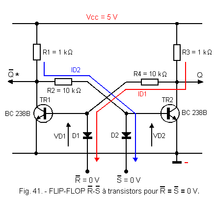
When the two entries ![]() and
and ![]() are in the state 1, the two diodes D1 and D2 are blocked and the two entries
are in the state 1, the two diodes D1 and D2 are blocked and the two entries ![]() and
and ![]() have no influence on the assembly.
have no influence on the assembly.
The transistors remain in the state where they were previously. It is thus the former states Qn - 1 and ![]() n
- 1 which are observed on Q and
n
- 1 which are observed on Q and ![]() .
.
We can say that the position ![]() =
= ![]() = 1 is the memory position of the assembly.
= 1 is the memory position of the assembly.
All this can be summarized in the truth table of Figure 42, the states of the outputs at the instant n being denoted Qn and ![]() n
and the states at the previous instant n - 1 denoted Qn - 1 and
n
and the states at the previous instant n - 1 denoted Qn - 1 and ![]() n
- 1.
n
- 1.
![]() 3. 2. 3. - BISTABLE COUPLED CROSSED MULTIVIBRATORS
MADE WITH NAND DOORS
3. 2. 3. - BISTABLE COUPLED CROSSED MULTIVIBRATORS
MADE WITH NAND DOORS
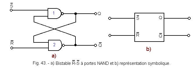
a) Description
The Figure 43-a represents the diagram of a rocker ![]() with doors NAND and Figure 43-b the symbol of a rocker
with doors NAND and Figure 43-b the symbol of a rocker ![]() .
.
b) Truth table
The truth table of this flip-flop is shown in Figure 44.
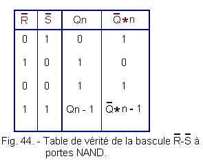
It is of course identical to that described for the flip-flop with discrete elements and seen in the previous chapter.
c) Operation
Figure 45 shows the operation of such a FLIP-FLOP. The entries ![]() (RESET) and
(RESET) and ![]() (SET) are active at the level L.
(SET) are active at the level L.
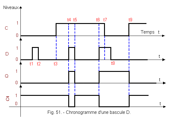
d) Chronogram of a rocker It is assumed at the beginning that the rocker is RESET,
This chronogram can be analyzed as follows : at time t1 :
at time t2 :
at time t3 : at time t4 : at time t5 :
at time t6 :
at time t7 : at time t8 : at time t9 : at time t10 : 3. 3. 1. MULTIVIBRATORS R.S.C. a) Description This is a NAND gate weighbridge whose inputs are controlled by two other NAND gates as shown in Figure 47. The «C» command input common to the two new NAND gates validates the two inputs R and S. These are called R and S because these inputs are active in state 1. When C is at state 1, the inputs S and R are enabled and the flip-flop R.S.C. becomes a conventional R-S flip-flop. When C goes to state 0, the entries If the exits Q and b) Chronogram of a flip-flop R.S.C.
(Figure 48). at time t0 : the flip-flop is RESET (Q
= 0, at time t1 : the input
SET goes to 1 but as the command input C is not at 1,
the flip-flop R.S.C. is in the memory position (that is to say that no change of state outputs does not occur). at time t2 :
S passes to 0, there is no change of the states of Q and of at time t3 :
R goes to 1 but C is not at 1, so no change of state of the outputs takes place. at time t4 :
R passes to 0, there is no change of the states of Q and of at time t5 :
S goes to 1 whereas C is to 1, the rocker thus becomes SET, Q passes to 1,
at time t6 :
S goes to 0, the previous state of the latch is stored that is to say that it remains SET
(Q = 1, at time t7 :
R goes to 1 while C is again to 1, the rocker becomes RESET (Q
passes to 0 and at time t8 :
R goes to 0, the previous state of the latch is memorized that is to say it remains RESET
(Q passes to 0, at time t9 :
S goes to 1 whereas C is always at 1, the rocker becomes SET
(Q passes to 1, at time t10 : S
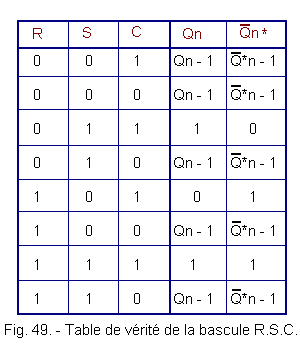
passes to 0, there is no change of the states of Q and of c) Truth Table The truth table in Figure 49 summarizes the operation of a R.S.C flip-flop. We note that each time C = 0, the latch is in the memory position whereas for C = 1, the flip-flop R.S.C. behaves exactly as a conventional R-S flip-flop. a) Description The R-S One R or The latch of type D or latch is derived from the latch R.S.C. It has, meanwhile, a single input «D» to position the outputs. In fact, an inverter is placed between the input S and the input R of the flip-flop R.S.C. The input S becomes the input D of the D type flip-flop whose diagram is shown in Figure 50. The exit When C = 1 and
D = 1, then When C = 1 and
D = 0, then When C goes to state 0, the flip-flop remains in the state where it was before the C input goes to 0, that is, it is SET or RESET. This is the memory position, the input D now has no action on the outputs Q and In summary, when C = 1, the output Q is in the same logical state as the input D. It is said that the output Q copies, reproduces (or follows) the input D (Q = D). When C goes to state 0, there is memorization output Q of the last logic present at the output Q so present at the input D. b) Chronogram of a D flip-flop (Figure 51). at time t1 : the data entry D passes to 1 but this entry is not taken into account, in fact, it is not validated by C (the exits Q
and at time t2 : the data input D returns to 0
but there is still no effect on the outputs because C = 0. at time t3 : the entry C passes to 1 but as D
is to 0, the rocker remains in position RESET (Q
= 0 and at time t4 :
D goes to 1, this change of state occurring when C = 1 is copied on the outputs of the latch so that it becomes
SET (Q = 1 at time t5 :
D returns to 0, this change of level, intervening when C = 1, is copied on the outputs of the rocker so that it becomes again RESET
(Q = 0 and at time t6 : D
goes to 1, the flip-flop becomes SET
(Q = 1 and at time t7 : C
goes to 0, the rocker goes to memory position at time t8 :
D goes to 0 but this change of state of the entry D is not taken into account by the rocker because C = 0. at time t9 : C
goes to 1 and as D is at 0, the output Q also goes to 0 : the flip-flop becomes RESET (Q
= 0 and c) Truth Table The truth table summarizing the functioning as it appears on the examination of the chronogram is represented in Figure 52. We can deduce from this truth table that every time C = 0, the latch memorizes the previous state of the outputs. In the case where C = 1, the output Q copies the input D : the flip-flop is SET for D = 1 and RESET for D = 0. With the flip-flop of type D or latch, the examination of the asynchronous circuits ends. In Theory 5 you will see the synchronous circuits and better understand the difference between these two families of sequential circuits.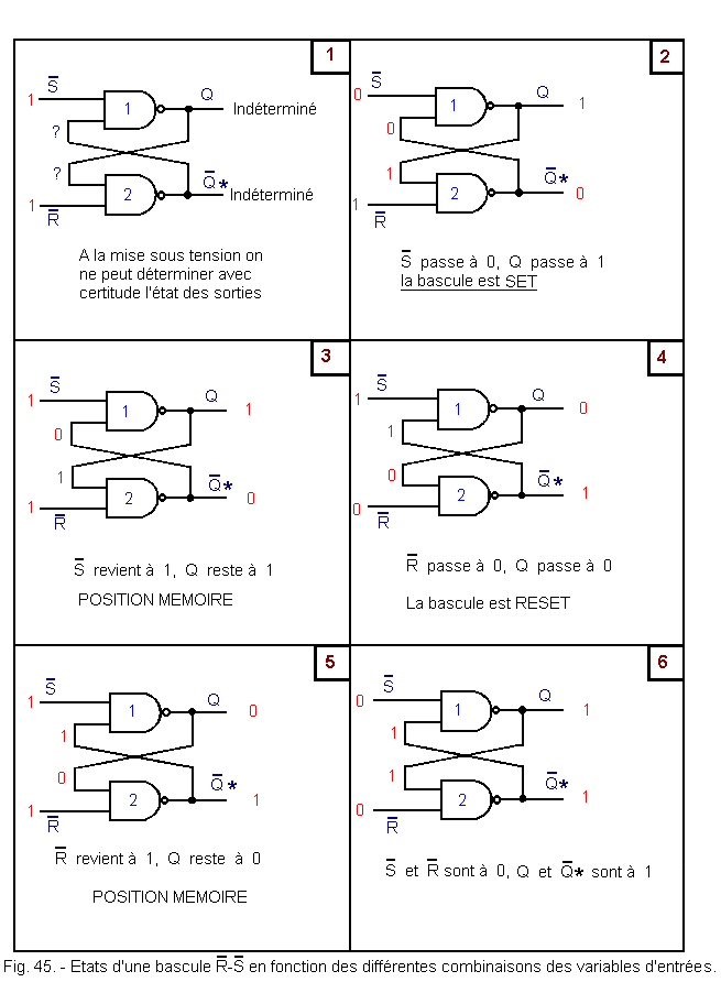
![]() with NAND doors (Figure 46).
with NAND doors (Figure 46).![]() and
and ![]() are at 1.
are at 1.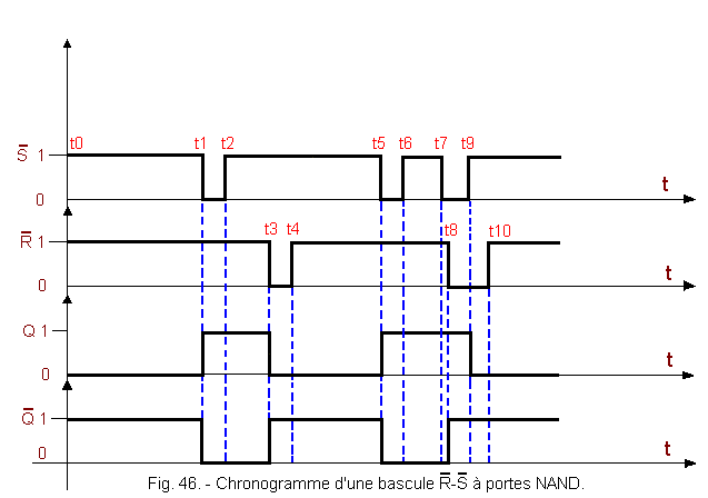
![]() passes to 0 which has the effect of making the toggle SET, Q goes to 1.
passes to 0 which has the effect of making the toggle SET, Q goes to 1.![]() goes back to 1, which has no influence. The rocker stays SET which means that it memorizes the previous action of
goes back to 1, which has no influence. The rocker stays SET which means that it memorizes the previous action of ![]() .
.![]() passes to 0 what has the effect of making RESET the rocker, Q passes to 0
and
passes to 0 what has the effect of making RESET the rocker, Q passes to 0
and ![]() passes to 1.
passes to 1.![]() goes back to 1 which has no effect, the rocker stays RESET which means that it memorizes the previous action of
goes back to 1 which has no effect, the rocker stays RESET which means that it memorizes the previous action of ![]() .
.![]() passes to 0 the rocker becomes SET, Q passes to 1 and
passes to 0 the rocker becomes SET, Q passes to 1 and ![]() passes to 0.
passes to 0.![]() passes to 1 the rocker rest SET.
passes to 1 the rocker rest SET.![]() passes to 0 the rocker being already SET, it remains SET.
passes to 0 the rocker being already SET, it remains SET.![]() passes to 0,
passes to 0, ![]() passes to 1 but Q remains at 1 because
passes to 1 but Q remains at 1 because ![]() is always at 0.
is always at 0.![]() passes to 1, Q passes to 0, the rocker is again RESET
because
passes to 1, Q passes to 0, the rocker is again RESET
because ![]() remained at 0.
remained at 0.![]() passes to 1, the rocker remains SET
which means that the previous action of
passes to 1, the rocker remains SET
which means that the previous action of ![]() is memorized.
is memorized.![]() 3. 3. - MULTIVIBRATORS DERIVED FROM CROSS-COUPLED MULTIVIBRATORS
3. 3. - MULTIVIBRATORS DERIVED FROM CROSS-COUPLED MULTIVIBRATORS 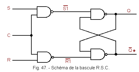
![]() 1
and
1
and ![]() 1
go to state 1 regardless of the state of the inputs S and R. Thus, the rocker
1
go to state 1 regardless of the state of the inputs S and R. Thus, the rocker ![]() goes to the idle state. It is the memory position, that is to say that the outputs Q and
goes to the idle state. It is the memory position, that is to say that the outputs Q and ![]() remain in the state where they were before the passage of the entry C to the state 0.
remain in the state where they were before the passage of the entry C to the state 0.![]() were both in the state 1, (
were both in the state 1, (![]() 1
=
1
= ![]() 1
= 0), the rocker RSC goes to the state and
1
= 0), the rocker RSC goes to the state and ![]() = 0) or in the state
0 (Q = 0 and
= 0) or in the state
0 (Q = 0 and ![]() = 1) according to the entry
= 1) according to the entry
![]() 1
or
1
or ![]() 1
which remained last in the state 0.
1
which remained last in the state 0.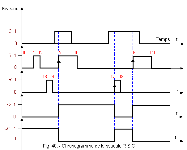
![]() = 1)
= 1)
![]()
![]() .
.
![]() passes to 0.
passes to 0.
![]() = 0).
= 0).
![]() passes to 1).
passes to 1).
![]() passes to 1).
passes to 1).
![]() passes to 0).
passes to 0).
![]() .
.
![]() 3. 4. - TYPE «D» OR «LATCH» ROCKET (LOCK IN ENGLISH)
3. 4. - TYPE «D» OR «LATCH» ROCKET (LOCK IN ENGLISH)![]() and R.S.C flip-flops examined previously had two inputs for positioning the flip-flop at a determined state.
and R.S.C flip-flops examined previously had two inputs for positioning the flip-flop at a determined state.![]() allowed to put the rocker to 0 (position RESET), the other
S or
allowed to put the rocker to 0 (position RESET), the other
S or ![]() allowed to put the rocker at 1
(position SET).
allowed to put the rocker at 1
(position SET).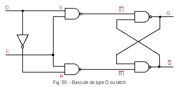
![]() becomes
becomes ![]() .
Indeed, in this rocker, the exits Q and
.
Indeed, in this rocker, the exits Q and ![]() are always complementary.
are always complementary.![]() 1
= 0 and
1
= 0 and ![]() 1
= 1. The flip-flop D is thus in state 1, (Q = 1 and
1
= 1. The flip-flop D is thus in state 1, (Q = 1 and ![]() = 0).
= 0).![]() 1
= 1 and
1
= 1 and ![]() 1
= 0. The flip-flop D
is thus in state 0, (Q =
0 and
1
= 0. The flip-flop D
is thus in state 0, (Q =
0 and ![]() = 1).
= 1).![]() .
.
![]() do not change of state.
do not change of state.
![]() = 1).
= 1).
![]() = 0) during the time when D is kept at 1.
= 0) during the time when D is kept at 1.
![]() = 1).
= 1).
![]() = 0) because C = 1
= 0) because C = 1
![]() = 1).
= 1).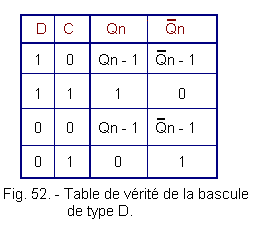
 Click here for the next lesson or in the summary provided for this purpose. Click here for the next lesson or in the summary provided for this purpose. |
 Top of page Top of page |
|
Previous Page |
 Next Page Next Page |
Nombre de pages vues, à partir de cette date : le 27 Décembre 2019

Envoyez un courrier électronique à Administrateur Web Société pour toute question ou remarque concernant ce site Web.
Version du site : 10. 4. 12 - Site optimisation 1280 x 1024 pixels - Faculté de Nanterre - Dernière modification : 02 Septembre 2016.
Ce site Web a été Créé le, 14 Mars 1999 et ayant Rénové, en Septembre 2016.