 NOR Function NOR Function
|
OU EXCLUSIVE Function
|
Verification of the operation of an EXCLUSIVE OR
|
|
NOR EXCLUSIF Function
|
Logical identity Function |
Footer
|
NAND function - NOR function - Exclusive OR function - NOR function Exclusive :
In this lesson, we will finish the review of basic logical functions such as NAND, NOR, OR EXCLUSIVE functions ... and solve some problems using the DE MORGAN theorems and the QUINE MAC CLUSKEY method.
1. - FUNCTIONS DERIVED FROM FUNDAMENTAL FUNCTIONS
1. 1. - NAND FUNCTION (NON - ET)
The NAND circuit, although derived from the AND circuit, is more used and more common than this one. Originally, it was technologically easier to make and less expensive, which explains why it was the most frequently used circuit. However, this is no longer quite true because advances in technology have seen the prices and performance of all circuits evolve very rapidly.
1. 1. 1. - THE NAND CIRCUIT
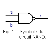
Its symbol is that of Figure 1.
A NAND circuit is obtained by putting in series an AND gate and an inverter as shown in Figure 2.
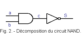
Let us study the relation existing between a, b and S ; for that, let's start from an AND circuit followed by an inverter circuit.
The truth table of the NAND circuit is obtained by first writing the equation c = a . b then S = ![]() .
.
The truth table of the circuit AND is represented Figure 3 :
.gif)
The truth table of the inverter circuit is reproduced Figure 4 :
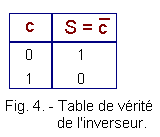
We can easily deduce the truth table of the NAND circuit which is represented in Figure 5 :
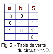
The output of a NAND circuit is in logic state 0 only when the two inputs are in state 1. It suffices that only one of the inputs is at 1 so that the output becomes 1.
The logical function NAND can be summarized by the equation Boolean ![]() according to the number of the entries.
according to the number of the entries.
We find the sign . symbolizing the product ET and the bar indicating the complementation.
1. 1. 2. - REPRESENTATION OF EULER (Figure 6)
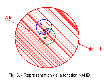
The AND function such that S = a . b is the intersection of A and B (blue hatched surface) while the inverse of a . b is ![]() is the set of red hatched surfaces.
is the set of red hatched surfaces.
1. 1. 3. - ELECTRICAL CIRCUIT (Return to the theory N° 3 TS)
Figure 7 represents the electric circuit used to carry out a NAND function with two input variables a and b, S being the output.
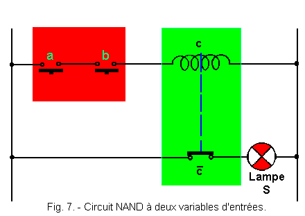
The contacts used a and b are working contacts, that is to say, open at rest. If we refer to theory 2, we see that the set represented in red is an AND realized with contacts so that a. b = C.
Now, C inside the set green is a relay whose coil is materialized by the sign ![]() .
It controls the contact
.
It controls the contact ![]() which is a rest contact so that one can write the operating table represented Figure 8.
which is a rest contact so that one can write the operating table represented Figure 8.
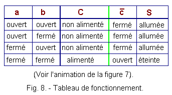
With the positive logical convention, one can write :
Closed contact = 1 ; open contact = 0
Lamp lit = 1 ; lamp off = 0
Relay powered = 1 ; relay not powered = 0
Hence the truth table shown in Figure 9 :
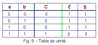
We see in this truth table that the output is always at 1 except for the two inputs at 1 or S = 0.
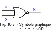
![]() 1. 2. - NOR FUNCTION
(Back to Theory N° 3 TS)
1. 2. - NOR FUNCTION
(Back to Theory N° 3 TS)
As for the AND gate which becomes, after addition of an inverter, a NAND gate, with an OR circuit followed by an inverter at its output, a NOR circuit is obtained whose graphic symbol is that of Figure 10-a :
The NOR circuit is equivalent to an OR circuit followed by an inverter as shown in Figure 10-b :
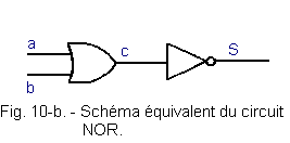
Let us study the existing relation between a, b and S, for that we start from an OR circuit followed by an inverter circuit.
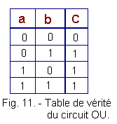
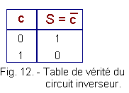
The truth table of the NOR circuit is obtained by first writing the equation C = a + b then
S = ![]() .
.
The truth table of the OR circuit is represented in Figure 11 :
The truth table of the inverter circuit is represented in Figure 12 :
The truth table of the NOR circuit can then be easily deduced (Figure 13) :
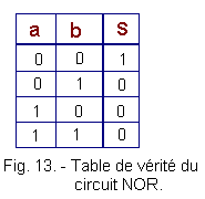
The output of a NOR circuit is at logic state 1 only when both inputs are at 0.
The logical function NOR can be summarized by the equation Boolean ![]() according to the number of the entries.
according to the number of the entries.
We find the sign + symbolizing the OR logical sum and the bar indicating the complementation.
1. 2. 1. - REPRESENTATION OF EULER (Figure 14)
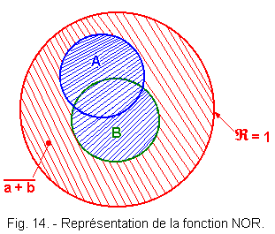
The OR function such that S = a + b is the union of A and B (blue hatched surface) while the inverse of a + b is ![]() is the set of red hatched surfaces.
is the set of red hatched surfaces.
1. 2. 2. - ELECTRICAL CIRCUIT
Figure 15 shows the electrical circuit used to perform a NOR function.
The contacts used a and b are working contacts, that is to say, open at rest. If we refer to theory 2, we see that the set represented in red is an OR realized with contacts so that a + b = C.
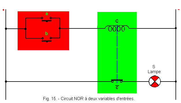
Now, C inside the hatched green set is a relay whose coil is materialized by the sign ![]() .
It controls the contact
.
It controls the contact ![]() which is a rest contact so that one can write the following operating table (Figure 16) :
which is a rest contact so that one can write the following operating table (Figure 16) :
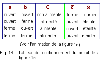
Given the positive logical convention, we can deduce the truth table from Figure 17 :
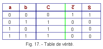
We see in this truth table that the output is always at 0 except for the two inputs at 0 or S = 1.
![]() 1. 3. - FUNCTION OU
EXCLUSIF (EXCLUSIVE OR)
1. 3. - FUNCTION OU
EXCLUSIF (EXCLUSIVE OR)
1. 3. 1. - TRUTH TABLE
The exclusive OR function is more complex than the set of functions we have just analyzed.
Recall the truth table of the inclusive OR function (Figure 18) :
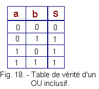
We see that the output S of the OR operator was at 1 when a OR b or both were at 1.
In the case of the exclusive OR, it will not be the same. Indeed, for S = 1, it will be necessary for a OU b to be exclusively 1, that is to say that S will not be at 1 when a and b are simultaneously at 1. The exclusive OR as its name is indicates excludes this possibility.
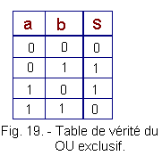
Figure 19 shows the exclusive OR truth table :
We then write that S
= a ![]() b that we state S equal a exclusive OR b.
b that we state S equal a exclusive OR b.
The symbol ![]() is the exclusive OR symbol in logical equations.
is the exclusive OR symbol in logical equations.
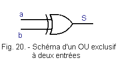
In the diagrams, the graphic symbol shown in Figure 20.
1. 3. 2. - REPRESENTATION OF EULER (Figure 21)
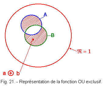
The exclusive OR function such that S = a ![]() b is the shaded area such that S = 1 for a = 1 or b = 1, that is the union of sets A and B excluding the common area at A and B.
b is the shaded area such that S = 1 for a = 1 or b = 1, that is the union of sets A and B excluding the common area at A and B.
1. 3. 3. - DIAGRAM WITH SIMPLE LOGIC OPERATORS
As we said at the beginning of this chapter, the exclusive OR function is more complex than the NAND or NOR functions.
Let's try by graphical reasoning to find an equation of S such that the sign ![]() disappears to bring the exclusive OR function back to classical AND and OR functions or inverse functions.
disappears to bring the exclusive OR function back to classical AND and OR functions or inverse functions.
We see that S is formed of two distinct surfaces :
-
- The S1 surface included inside A
-
- The S2 surface included inside B.
Figure 22 shows the area S1.
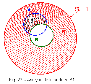
The set ![]() hatched in red is the complement of B with respect to Â.
hatched in red is the complement of B with respect to Â.
We see that the surface S1, represented by the vertically hatched set in black, is the intersection of ![]() and of A.
and of A.
We can therefore write S1 = a![]() because if A and B are the sets for which a and b are respectively at 1, S1 will be the set for which a = 1 and b = 0.
because if A and B are the sets for which a and b are respectively at 1, S1 will be the set for which a = 1 and b = 0.
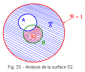
We can easily by following the same reasoning to see in figure 23 that S2 = ![]() b
since S2 is the intersection of
b
since S2 is the intersection of ![]() and of B.
and of B.
From the truth table of the exclusive OR function (Figure 19), we can establish the karnaugh table of this function represented in Figure 24.
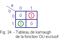
In this respect, it is absolutely fundamental to remember how one realizes a karnaugh painting from the truth table.
The values of the output S for a given combination of a and b are plotted in the box at the intersection of the values of a and b considered, carried on the sides of the table. We advise you to come back to theory 2 if necessary to review the karnaugh tables.
We can deduce :
-
red group S = a
 ,
, -
green group S =
 b,
b,
From where we can write :
S = ![]() b
+ a
b
+ a![]()
This confirms the result obtained by the graphical decomposition realized thanks to the representation of Euler.
We can now construct the scheme of Figure 25 which represents an exclusive OR function performed from AND, OR and NO functions.
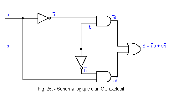
![]() 1. 3. 4. - VERIFICATION OF FUNCTIONING FROM THE LOGIC DIAGRAM AND RECONSTITUTION OF THE TRUTH TABLE
1. 3. 4. - VERIFICATION OF FUNCTIONING FROM THE LOGIC DIAGRAM AND RECONSTITUTION OF THE TRUTH TABLE
In Figures 26 a, b, c and d are shown the four combinations that can be taken by two inputs a and b.
On each of these Figures are reported the different logical levels at the entrance and exit of each door.
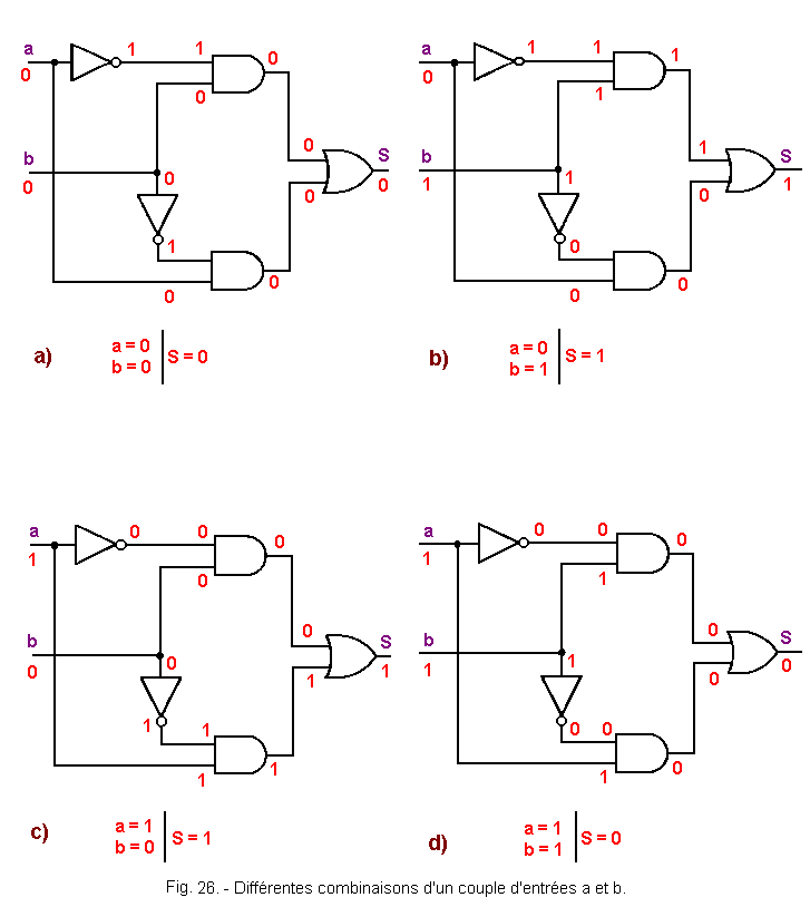
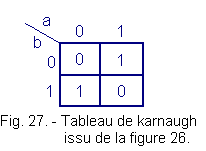
We can recapitulate the four cases of Figure 26 in the Karnaugh table of Figure 27. The resulting table corresponds in all respects to the table of the exclusive OR function.
This last exercise may have seemed useless to you, in reality it is not so because it is necessary to feel perfectly at ease in the tables of Karnaugh, truth tables and diagrams in order to be able to make the transformation in a meaning or in the other without error and possibly during the development of a complex circuit to be verified using each time a different method.
![]() 1. 4. - EXCLUSIVE NOR
FUNCTION (EXCLUSIVE NOR)
1. 4. - EXCLUSIVE NOR
FUNCTION (EXCLUSIVE NOR)
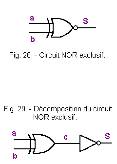
The exclusive NOR circuit shown in Figure 28 is identical to NAND and NOR, but using an exclusive OR circuit followed by an inverter (Figure 29).
The logical equation of the two-input exclusive NOR is ![]() .
This equation indicates that the exclusive NOR performs the exclusive OR operation and complements the result (bar above).
.
This equation indicates that the exclusive NOR performs the exclusive OR operation and complements the result (bar above).
You can use the process followed for the NAND and NOR doors yourself to find the truth table. We will confine ourselves to indicating this table, figure 30, for an exclusive NOR with two entries.
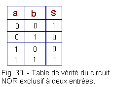
An exclusive NOR circuit, such as an exclusive OR circuit, is used to detect the presence of a single signal either a or b (it is said that the signal a or b is present when it has a logic level 1).
In the case of the exclusive NOR circuit, one can also check the equality between two signals a and b. Indeed, S is 1 for a and b simultaneously at 1, but also for a and b simultaneously at 0.
![]() 1. 5. - LOGICAL IDENTITY FUNCTION
1. 5. - LOGICAL IDENTITY FUNCTION
The logical identity function does not exist as such in the form of integrated circuits. However, it can render services in some automation to create security.
Suppose, for example, that on the one hand a variable a indicates the direction of rotation of a motor (a = 1 "forward", a = 0 "reverse") and, on the other hand, for reasons of safety one must check that a tool is correctly positioned on the machine according to the direction of rotation chosen (b = 1 "size before", b = 0 "size back").
It can be seen immediately that for reasons of safety, it is necessary that the start-up be authorized only for a = b = 1 OR for a = b = 0. The materialization of the authorization of start-up will be realized for example by means of 'a lamp.
The equation of such a logical identity is :
S = ab + ![]()
![]()
That we write :
S = a ![]() b
b
Figure 31 gives the electrical diagram of this logical identity made with contacts.
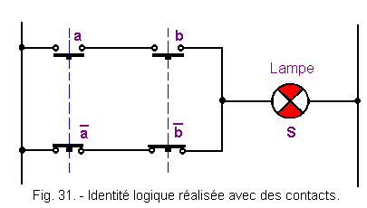
You now know that an AND is materialized by serial contacts and an OR by parallel contacts.
The row of contacts work a, b materializes therefore ab whereas the row of contacts rest materializes
![]()
![]() .
The two rows of contacts being in parallel, we have :
.
The two rows of contacts being in parallel, we have :
S = ab + ![]()
![]()
Figure 32 gives the electrical diagram of the same logical identity but this time made using electronic gates.
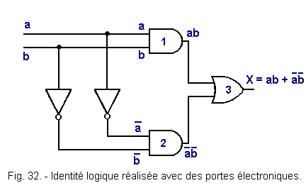
The realization of such a scheme is even simpler, we establish ab and ![]()
![]() by means of two AND gates (respectively gates n° 1 and n° 2),
by means of two AND gates (respectively gates n° 1 and n° 2), ![]() et
et ![]() being obtained previously by two inverters.
being obtained previously by two inverters.
The OR circuit (gate n° 3) carries out the final operation to obtain :
S = ab + ![]()
![]()
We will now study the negative logic and the theorem of DE MORGAN on another page so as not to clutter it.
 Click here for the next lesson or in the summary provided for this purpose. Click here for the next lesson or in the summary provided for this purpose. |
 Top of page Top of page |
|
Previous Page |
 Next Page Next Page |
Nombre de pages vues, à partir de cette date : le 27 Décembre 2019

Envoyez un courrier électronique à Administrateur Web Société pour toute question ou remarque concernant ce site Web.
Version du site : 10. 4. 12 - Site optimisation 1280 x 1024 pixels - Faculté de Nanterre - Dernière modification : 02 Septembre 2016.
Ce site Web a été Créé le, 14 Mars 1999 et ayant Rénové, en Septembre 2016.