 Programmable Logic Networks Programmable Logic Networks |
PLA "Programmable Logic Array"
|
The FPLA
|
|
FPLA with Memory
|
Footer |
Programmable Logic Networks - "PLA" - FPLA :
In the previous theory, we saw the use that we could make of the ROM memories, to replace a combinatorial circuit formed generally with logic gates NAND, NOR, ...
This technological evolution in the direction of programmable circuits, already noted during the examination of the multiplexers, led the manufacturers of integrated circuits to realize other programmable logic devices known under the name PLA (Programmable Logic Array).
PLA, as well as multiplexers, demultiplexers and microelectronic memories, are the result of recent integration technologies, which have also led to the design and realization of very complex circuits such as microprocessors and their associated circuits.
This evolution towards circuits with a high level of integration has also posed new problems related to the assembly of integrated circuits with each other and their interfacing which is the set of principles and techniques for connecting several electronic systems together.
In this theory, we will give a general view on these recent circuits, as well as on all the related problems.
![]() 1. - PROGRAMMABLE LOGIC NETWORKS
1. - PROGRAMMABLE LOGIC NETWORKS
1. 1. - COMPLEX INTEGRATED CIRCUITS
The level of integration of circuits continues to grow and we agree to recognize the following categories of integrated circuits :
![]() S.S.I.
(Short
Scale
Integration) : 1 to 10 transistors per integrated circuit.
S.S.I.
(Short
Scale
Integration) : 1 to 10 transistors per integrated circuit.
![]() M.S.I.
(Medium
Scale
Integration) : 10 to a few hundred transistors.
M.S.I.
(Medium
Scale
Integration) : 10 to a few hundred transistors.
![]() L.S.I.
(Large
Scale Integration) : from a few hundred to 10 000 transistors.
L.S.I.
(Large
Scale Integration) : from a few hundred to 10 000 transistors.
![]() V.L.S.I.
(Very
Large
Scale
Integration) : more than 10 000 transistors.
V.L.S.I.
(Very
Large
Scale
Integration) : more than 10 000 transistors.
The evolution of integrated circuits has been such that the cost per integrated transistor has been reduced over the last twenty years to one millionth of that initially.
It is now possible to focus on a single integrated circuit a whole set of logical functions formerly performed by several integrated circuits. Think of office calculators for example : towards the end of the sixties, we started to build them with dozens of circuits S.S.I. and M.S.I. ; today, only one integrated circuit L.S.I. perform all necessary operations.
It is because these calculators can be distributed to several tens of thousands of copies that it has appeared more advantageous to design and produce a single integrated circuit grouping all the functions of the calculator.
Generally, the builder buys the necessary integrated circuit (s), mechanical and electrical accessories, displays and final assembly of these various elements to build these calculators.
The same procedure is usually followed for the manufacture of digital watches.
For small series production, a manufacturer may employ other methods, in particular using standard components.
The determining factor is the quantity of a given product that will be sold on the market. In general, when this quantity is large enough, the manufacturer has an appropriate circuit (or several) made by an integrated circuit manufacturer.
These integrated circuits are called CUSTOM (client) because they are developed at the request of a specific customer.
The first microprocessor was created this way.
For small series production, the most economical solution is to use the standard components available on the market. In some cases, there are several solutions for performing a function. For example, one can either design a combinatorial network, or use ROM or multiplexers, as has been indicated in previous theories.
In general, it is preferable to use more complex integrated circuits in small numbers rather than a large amount of less complex integrated circuits. Indeed, the cost price of a complex circuit (for example L.S.I.) is only slightly higher than that of a simple circuit (S.S.I.).
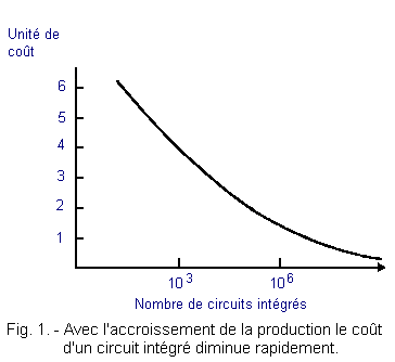
It should be noted, moreover, that a circuit L.S.I. can be significantly more expensive than a S.S.I circuit. in the first phase of production of this circuit because the cost is directly related to the quantity produced. As shown in Figure 1, the cost price decreases very rapidly when production increases.
Complex integrated circuits therefore have several advantages ; they can replace several less complex integrated circuits, they reduce the size of printed circuits, facilitate assembly operations and ultimately reduce the cost.
We can also note that in the overall cost of a microelectronic system, the price of integrated circuits represents about 10% of the total amount, the remaining 90% being divided between the following different items :
-
Printed circuit board,
-
Connectors,
-
Insertion and soldering of integrated circuits,
-
Liaisons,
-
Supply,
-
Frame,
-
Decoupling capacitors,
-
System test,
At this manufacturing cost are added the costs relating to the study of the electronic system, the storage of finished products and system components, the administration, etc.
It has been calculated that the sum of all costs, in the case of an average digital system, is about twenty times the cost of the integrated circuits making up this system. If for example, the price of the component is one euro, the total cost will be twenty euros.
So the total cost of a system is a function of the number of integrated circuits that compose it even if it is not directly proportional to it.
On the graph in Figure 2, we see that a system composed of 200 integrated circuits costs 2 units and that requiring 800 integrated circuits is 4 units.
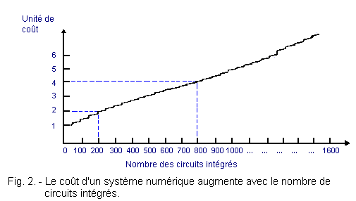
The number of integrated circuits is multiplied by 4 while the cost of the system doubles only.
If now the two systems were integrated in a single circuit, their overall costs would be roughly equivalent since the two integrated circuits would return at almost the same price.
These different concepts are well known to integrated circuit producers and their customers. Nevertheless, there is a disadvantage : complex integrated circuits are very specialized and very varied. As a result, they are generally produced in smaller quantities than standard circuits.
Under the pressure of these different problems, attempts have been made to design circuits with a high level of integration, but which can fulfill a wide variety of functions. This led to the design of PLA or Programmable Logic Networks.
![]() 1. 2. - PROGRAMMABLE LOGIC NETWORKS (PLA)
1. 2. - PROGRAMMABLE LOGIC NETWORKS (PLA)
PLA have been designed on the premise that any logical function can be written as a sum of minterms (canonical form). For example, the function F = ![]() bd
+ ab
bd
+ ab![]()
![]() + a
+ a![]() cd.
cd.
This function is the sum of the following three mintermes : ![]() bd,
ab
bd,
ab![]()
![]() and a
and a![]() cd.
cd.
PLA can generate a number of mintermes from n variables and sum these minterms.
Figure 3 shows the basic structure of a PLA.
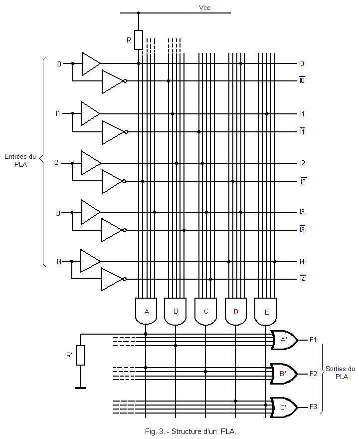
Each five-input AND gate (A, B, C, D, E) makes it possible to generate a mint from the five input variables (I0, I1, I2, I3, I4).
Each four inputs OR gate (A', B', C') makes it possible to sum the minterms necessary to obtain a defined logic function.
The circuit is arranged in matrix form with horizontal and vertical links.
In the upper part, the horizontal lines represent the inputs I0, I1, I2, I3 and I4 of the PLA and the vertical lines correspond to the inputs of the AND gates.
Initially, the horizontal and vertical lines intersect without contact between them. The programming will consist in later joining a horizontal line with a vertical line at a junction point symbolized in Figure 3 by a point.
The logical state of the output of an AND gate therefore corresponds to the value of a minterme.
It will be sufficient, during programming, to bring together the outputs of the AND gates that are desired at the inputs of the OR gates in order to realize the logical sum of these minterms.
In the example of Figure 3, three «combinatorial networks» have thus been «created» ; their respective outputs being the three outputs F1, F2 and F3.
The circuit having for output F1 is formed with the OR gate (A') and with the AND gates A and B ; that having F2 output is formed with the doors B', A and C ; finally, the one having F3 output is formed with the doors C', D and E.
Figure 4 shows the first of these three combinational circuits.
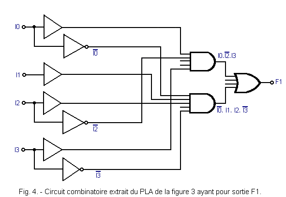
The logical function F1 is written :
![]()
As a general rule, PLA programming is done by the manufacturer from the data provided by the customer.
The latter, for example, can provide an operating table relating to the problem to be solved.
We will examine a deliberately simple example from the table in figure 5.
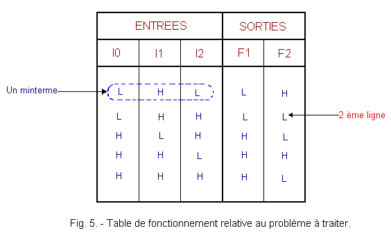
It is necessary to constitute five mintermes. So you need at least five AND gates with three inputs (there are three variables). It also requires two OR gates since there are two functions (F1 and F2) to generate.
The PLA programmed to answer the problem is given in Figure 6.
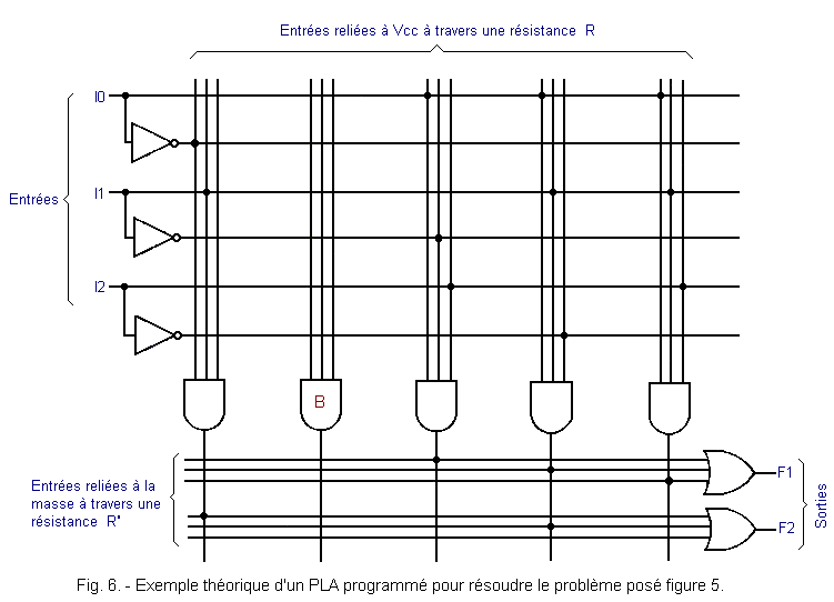
Note that the AND noted B is not used. Indeed, in the operating table of Figure 5, in the second line, you see that the two outputs F1 and F2 are in the L state, so it is not necessary to wire the inputs of the door B.
Finally, four AND gates are sufficient to solve the problem.
It would be possible to solve this problem by using a ROM. Theoretically, it would require a ROM with three inputs and two outputs is a ROM whose capacity would be 23 (combinations possible with three inputs) multiplied by 2 (number of outputs), 8 x 2 = 16 bits.
In the case of a PLA, one defines the capacity of matrix which is equal to the product of the number of doors AND by the number of OR gates. This capacity is expressed in bits. In this case, it is 4 x 2 = 8 bits.
The advantage of PLA over ROM is evident from the 14 inputs and 8 outputs PLA available on the market.
Consider a PLA with 96 AND gates, which already allows many possibilities, for example the constitution of 96 mintermes. The matrix capacity of this PLA is 96 x 8 = 768 bits.
An equivalent ROM should have a capacity of 214 x 8 = 131 072 bits.
A PLA is therefore much more advantageous than a ROM. Indeed, in the case of the latter, it is necessary to take into account all the possible combinations of the entries : with 14 entries, , it is necessary a ROM with 214 = 16 384 addresses, whereas with a PLA one is only interested in to the combinations given by the operating table that are necessary to solve the problem.
![]() 1. 3. - THE FPLA
1. 3. - THE FPLA
As manufacturers designed and produced PROM after ROM, Field Programmable Logic Array (FPLA) appeared after PLA.
Their principle remains the same as that of the PLA. FPLA are easily programmable by the user. All that is needed is a device to program which is often a simple PROM programmer.
The principle of programming these FPLA is to melt fuses in the appropriate places by passing through a short current overcurrent, exactly as you do with PROM.
Figure 7 shows the diagram of an already programmed FPLA. The fuses are represented by the symbol ![]() .
.
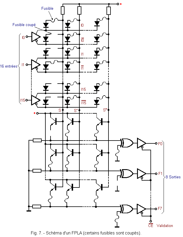
The represented FPLA has 16 entries rated I0 to I15 and 8 outputs noted F0 to F7.
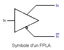
For each FPLA entry, there are two horizontal lines ; the signal present on one being complementary to the one present on the other, as indicated by the following symbol :
The point S (as well as S', S" ...) is the output of an AND consisting of diodes in parallel.
If one wants to represent the first AND of FPLA, one obtains the diagram of Figure 8.
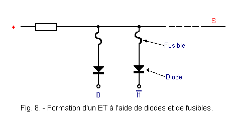
This first minterme can be written as well :
S = I0 . ![]() 1
1
In the same way, the second minterme (exit S') will be written :
S' = I0 . ![]() 0
. I1 .
0
. I1 . ![]() 1...
I15 .
1...
I15 . ![]() 15
15
It is obvious that S' = 0 for all combinations of the input variables.
OR consist of transistors in parallel. The first OR corresponding to the output F0 can be represented as shown in Figure 9.
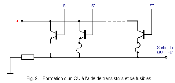
The output F0' of the OR is equal to F0' = S' + S".
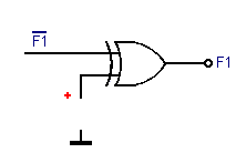
The Exclusive OR gate is used to invert the output signal of the corresponding OR. It suffices to melt the fuse and this input is then at logic H. This is the case of the F1 output (Figure 7).
Example :
There is an entry of command noted ![]() (initials of Chip Enable = validation of box). It validates the eight outputs when it is at level L. On the other hand, when this input is at level H, the eight outputs are in the high impedance state (tri-state outputs).
(initials of Chip Enable = validation of box). It validates the eight outputs when it is at level L. On the other hand, when this input is at level H, the eight outputs are in the high impedance state (tri-state outputs).
![]() 1. 4. - FPLA WITH
MEMORY
1. 4. - FPLA WITH
MEMORY
Another type of logical network has also developed, the FPLA with memory.
This FPLA has a register, generally consisting of a set of RS type synchronous flip-flops.
This register enables the installation in the FPLA of a sequential logic circuit. The state of the outputs is both a function of the state of the inputs and the logic state of the outputs before the clock edge.
The block diagram of Figure 10 represents a FPLA with memory.
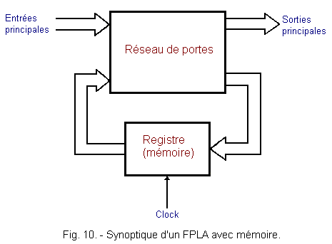
Thanks to the register, the data present at the output of the FPLA are reintroduced at the entrance of the gate network at the next clock edge.
The diagram of Figure 11 is a more developed synoptic of a FPLA with a memory called FPLS (Field Programmable Logic Sequencer).
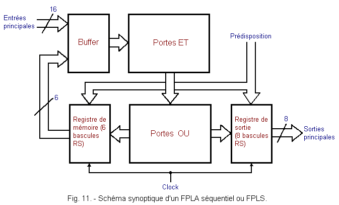
The buffer is a logical set that collects both the data on the 16 main inputs and the 6 outputs of the storage register.
The output register serves to hold the data between two clock pulses.
There is also the network of AND and OR doors characteristic of PLA.
1. 5. - GATE ARRAY
Sometimes the PLA described in the previous paragraphs are unsuitable for solving certain problems ; either that they are not flexible enough to use, or that a large number of fairly complex circuits must be made.
A first solution is to design customs or specific integrated circuits.
A second solution is to use circuits whose principle is intermediate between that of the PLA and customs and that is called Gate Array (logic gate network) or FPGA (Field Programmable Gate Array).
These circuits consist of a large number of NAND gates generally between 500 and 2000.
The technology used is either TTL S (Schottky) technology or CMOS technology.
Programming involves connecting NAND gates together to form the appropriate logical network.
The advantage of the Gate Array is that it can be produced on a large scale for a variety of applications.
An integrated circuit of this type can replace up to 50 S.S.I integrated circuits and M.S.I.
The Gate
Array,
as the PLA is programmed by the constructor from the specific problem proposed by the customer. All the circuits we have just seen, FPLA, FPLS, and FPGA are sometimes called IFL (Integrated Fuse Logic).
 Click here for the next lesson or in the summary provided for this purpose. Click here for the next lesson or in the summary provided for this purpose. |
 Top of page Top of page |
|
Previous Page |
 Next Page Next Page |
Nombre de pages vues, à partir de cette date : le 27 Décembre 2019

Envoyez un courrier électronique à Administrateur Web Société pour toute question ou remarque concernant ce site Web.
Version du site : 10. 4. 12 - Site optimisation 1280 x 1024 pixels - Faculté de Nanterre - Dernière modification : 02 Septembre 2016.
Ce site Web a été Créé le, 14 Mars 1999 et ayant Rénové, en Septembre 2016.