A Pseudo-Monostable - A True Monostable Circuit 74C74 :
This practice allows you to study monostable circuits. These are quite often used in the design of digital circuits. These monostables cover both digital electronics and analog electronics.
The flip-flops can have two stable states and move from one state to another thanks to an external command. On the other hand, the monostable is characterized by a single state of stability.
This monostable circuit can go to an unstable state under the effect of an external command. It will remain in this state of instability for a duration depending on the characteristics of the circuit, then return to the stable state of departure.
Integrated monostable circuits are often used to increase the duration of a short signal, or to create a delay. Their principle is based on a time constant realized by means of a cell R.C. (resistance and capacitor).
1. - PREPARATION OF EQUIPMENT
In this practice, you will use the following components, which you will take from the material in your possession :
1 integrated circuit MM 74C08
1 integrated circuit MM 74C04
1 integrated circuit MM 74C74
1 integrated circuit MM 74C221
1 integrated circuit CD 4528
1 integrated circuit MM 74C85
2 diodes 1N 4148
1 tantalum electrolytic capacitor 0,33 µF - 10 V
1 tantalum electrolytic capacitor 0,47 µF - 10 V
2 tantalum electrolytic capacitor 1 µF - 10 V
1 tantalum electrolytic capacitor 10 µF - 10 V
2 resistors of 1 MW
- 1 / 4 W tolerance ±
5 % (brown - black - green - gold)
1 resistance of 2,2 MW
- 1 / 4 W tolerance ±
5 % (red - red - green - gold)
2 resistors of 220 kW
- 1 / 4 W tolerance ±
5 % (red - red - yellow - gold)
2 braids of insulated tinned wire (one red, one black).
2. - FIRST EXPERIENCE : USE OF A PSEUDO-MONOSTABLE TO GENERATE PULSES OF DURATION GIVEN
You have seen that the control signal of a digital circuit can be constituted by the pulse generated by the pushbuttons mounted on the desk.
The duration of this control signal corresponds to the time during which the push button is depressed.
This type of control signal is not always appropriate. Indeed, some digital circuits require a control signal of definite duration.
Monostable integrated circuits are used for this purpose.
You will now examine the simplest of monostable circuits called pseudo-monostable because it is an imperfect monostable circuit.
Start the experiment now by mounting the circuit, following the instructions below.
2. 1. - REALIZATION OF THE CIRCUIT
a) Make sure that the power supply is disconnected and remove from the matrix and the group of connectors all the connections previously established as well as the ICX integrated circuit.
b) Perform the assembly as shown in Figure 1-a, as follows :
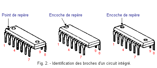
make sure the correct orientation of the integrated circuit MM 74C04. All integrated circuits are identified by a notch or a point as shown in Figure 2.
Pin 14 is connected to the positive voltage.
Pin 7 is connected to the negative voltage (ground).
The resistance R1 of 1 MΩ 1 / 4 W tolerance 5% (brown - black - green - gold) is connected between pin 1 and ground.
Pins 2 and 3 are connected together.
Pin 4 is connected to contact L0 of the connector group.
Insert on the matrix the tantalum electrolytic capacitor C1 of 1 µF - 10 V between pin 1 of the integrated circuit and a contact on the left of the integrated circuit.
For the moment, do not insert the second capacitor in dotted line.
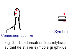
You must respect the polarity of C1. The positive terminal is marked with the sign (+) as shown in Figure 3.
The positive connection of C1 is connected to SW0 by a connecting wire, while the negative connection of C1 is connected to the pin 1 of the integrated circuit MM 74C04.
Once assembly is complete, check the accuracy of the connections made (Figures 1-a and 1-b).
2. 2. - OPERATING TEST
a) Connect the power supply.
La LED L0 is off.
If this is not the case, carefully check the entire assembly. Note, however, that when the power is turned on, the LED may come on briefly.
b) Set switch
SW0
to position 1.
The LED lights up for about 1 second and then goes off, switch SW0 is always in position 1. Repeat the experiment, always starting from position 0 for SW0. The LED always comes on for about 1 second.
c) Switch SW0 to position 0. Set SW0 to position 1 and return SW0 quickly to position 0. The LED goes out as soon as SW0 is reset to position 0, even if it has not been switched on for 1 second.
This is the main limit of use of the circuit. Indeed, it is necessary that the control pulse generated by SW0 lasts at least as long as the duration of the output pulse.
In the opposite case, the output pulse of the circuit will only last for the time during which the switch is in position 1.
Similarly, after returning to the 0 position for SW0 by reducing the duration of the output pulse, you put SW0 back to position 1. You will notice that the output pulse will still be less than 1 second.
d)Now
take another 1 µF - 10 V tantalum electrolytic capacitor (C2) and insert it with the polarities of the terminals in parallel with the first capacitor C1,
as shown in Figure 1-a dotted line.
The equivalent capacitance of the two capacitors is 2 µF.
e) Actuate the switch SW0. You notice that the output pulse lasts about twice as long as the output pulse of the previous test.
So the duration of the pulse increases with the capacity.
f) Remove C2, inserted last. There remains only C1, of value of 1 µF and replace the resistance of 1 MΩ (R1) by another resistance of 2.2 MΩ.
Repeat the test. You also notice that the LED lights up for about 2 seconds.
An approximate value of this pulse duration called T is given by the product RC.
T = RC
(T
in second,
R in Ohmand C
in Farad)
With a capacitor having a capacitance C = 1 µF = 1 x 10⁻⁶
F and a resistance
R = 1 MW
= 1 x 10⁶ W
the time T
is equal to :
T = 1 x 106
x 1 x 10-6 = 1 s
This value is the one obtained experimentally with the assembly. In fact, you do not get this value exactly because many of the characteristics of the components (resistance, capacitance, inverter) are not taken into consideration.
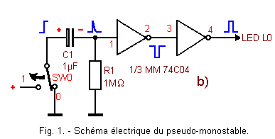
In the assembly, you used two inverters while only one would have been sufficient for the pseudo-monostable test.
In fact, the second inverter allows us to turn on the LED during the output pulse. The waveforms shown in the diagram of
Figure 1-b represent the pace of the voltage at different points of the circuit, as it would appear on the oscilloscope.
Switching SW0 to position 1 delivers a positive pulse on capacitor C1. At the input 1 of the diagram, there is also a positive pulse which decreases gradually. At output 2, you have the negative pulse that lasts 1 second (or 2 seconds) and output 4, the same inverted pulse.
3. - SECOND EXPERIENCE : EXAMINING
A PSEUDO-MONOSTABLE COMMANDED BY A DESCENDING FRONT
The circuit relating to this experiment is very similar to the previous one, as you can see in Figure 4.
It differs only by the resistor R1, here connected to the positive voltage, by the absence of the second inverter and finally by the inversion of the terminals of the capacitor C1.
You will mount the circuit using the wiring diagram and then check the operation by following the same procedure as in the previous experiment.
Disconnect the power supply. Remove the R1 terminal connected to the negative voltage and connect it to the positive voltage. You connect the output 2 of the first inverter to the contact L0.
Do not forget to invert capacitor C1.
In this experiment, SW0 will be in the initial position on 1. After verifying the accuracy of the wiring, connect the power supply and switch SW0 to position 0. The LED L0 comes on for about 1 second with R1 = 1 MΩ and C1 = 1 µF and about 2 seconds with R1 = 2.2 MΩ and C1 = 1 µF.
The only difference from the previous experiment is that you apply a negative pulse to the input 1 of the inverter. This assembly avoids the use of a second inverter.
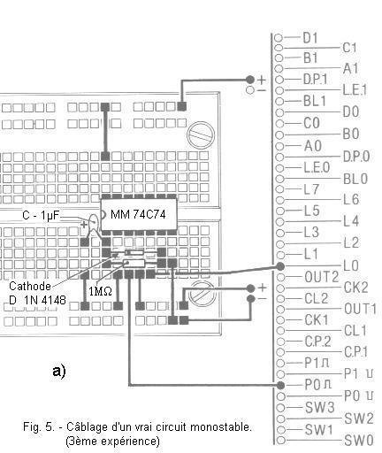
4. - THIRD EXPERIENCE : EXAMINING A TRUE
MONOSTABLE CIRCUIT
The pseudo-monostable circuits previously seen are not able to provide longer output pulses than the control pulse.
By using a flip-flop D and the cell comprising a resistor, a capacitor and a diode, you are now experiencing a true monostable circuit, the duration of the output pulse not depending on the duration of the control pulse.
b) Remove all components and links related to the previous experiment.
c) Carry out the assembly shown in Figure 5-a, using an integrated circuit MM 74C74 (including two flip-flops D), a resistance of 1 MΩ, a capacitor of 1 µF and a diode of type 1N 4148.
Do not disconnect the integrated circuit MM 74C00 in the IC1 support (debounce circuit).
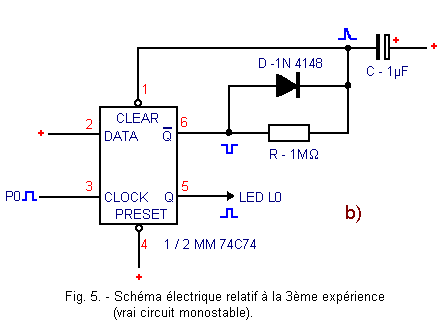
You have thus realized the schematic circuit in Figure 5-b.
The CLOCK input is connected to the P0 contact.
Output Q is connected to contact L0.
4. 2. - OPERATING TEST
a) Connect the power supply. L0 is off or stays on for a short while before turning off.
b) Press the P0 button. LED L0 lights for 1 second. The Q output is thus changed to the H state for 1 second.
c) Immediately press and release P0. LED L0 always lights up for 1 second.
It is therefore no longer necessary to press P0 for more than one second, but a brief pulse is sufficient to control the circuit.
Let's now examine the operation of this circuit using Figure 5-b.
The rising edge of the clock signal allows the transfer of the data DATA to 1 at the output Q.
Proceed therefore at the level L. The capacitor The output C thus loads through the resistor The output R. The voltage present at the input CLEAR decreases and when this voltage reaches a threshold low enough, the entry CLEAR is activated.
The output Q
goes to 0 and
to 1. The time required to activate CLEAR is a function of the time constant RC. When is high, the diode D is forward biased and allows the fast discharge of the capacitor C. The CLEAR input returns to the initial potential in the high state.
The circuit is found in the initial conditions of rest.
You will try to change the value of the resistor and capacitor (capacitor paralleling and also resistance).
The illumination time of the diode L0 is always equal to about the time constant RC.
In conclusion, the true monostable circuit has the following characteristics :
it generates a pulse of definite duration each time a rising edge is applied to the CLOCK input.
the duration of the output pulse depends solely on the values of R and C.
the control signal can immediately fall back to the L level without changing the shape and duration of the output signal.


 Examination of a pseudo-monostable
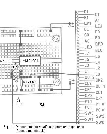
.gif)
 Click here for the next lesson or in the summary provided for this purpose.
 Top of page
 Next Page