7. - FOURTH EXPERIENCE : "ROCKET D IN A CIRCUIT USED FOR THE SIGNALING OF A FIRST EVENT"
With the experiments conducted so far, you have had the opportunity to examine the operation and characteristics of different types of integrated circuits. These were the combinational logic circuits AND, NAND, NOR, OR, OR-EXCLUSIVE, inverters and flip-flops.
These experiments were necessary in order to know the basic components used in digital circuits. It may have seemed monotonous to you, as well as the learning, though necessary to solve the problems, of the four fundamental operations at school.
When you have discovered the possibilities of practical applications, digital electronics will become captivating.
With your knowledge of basic logical integrated circuits, you are able to make practical circuits, simple at first, then more complex.
With a D flip-flop, you will perform a circuit that will detect the push-button depressed first.
A circuit of this type finds an application for example in game shows, to indicate which of the two players pressed the first button.
In the industrial field, it is necessary to determine which event occurs before another.
7. 1. - REALIZATION OF THE CIRCUIT
a) Disconnect the power supply and remove from the matrix and the group of connectors all the connections and the integrated circuit assembled during the previous experiment.
b) Take an integrated circuit MM 74C74 (double D flip-flop) and MM 74C08 (quadruple AND) and insert them on the matrix in the position shown in Figure 20-a.
c) Make the connections also shown in Figure 20-a.
d) Set the SW0 switch to the 0 position.
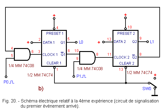
By observing the wiring diagram of the circuit carried (Figure 20-b) you see this :
the DATA inputs of the two flip-flops are wired to the positive voltage, so a positive transition on the CLOCK clock input transfers a logic level 1 to the Q output.
the CLEAR inputs are connected together to the switch SW0. Just put it on position 0 to have a logical level 0 on both outputs Q1 and Q2.
the PRESET inputs are wired at the positive voltage and therefore have no influence on the operation of the flip-flops.
The CLOCK inputs are connected through two AND circuits to the P0
and P1.
the outputs Q1 and Q2 respectively control the LEDs L0 and L1.
7. 2. - CONTROL OF OPERATION
a) Connect the power supply. You notice that both LEDs L0 and L1 are off. Indeed, SW0 is on the 0 position and the two CLEAR inputs are active ; the outputs Q1 and Q2 are therefore at the level L.
b) Set SW0 to position 1 : CLEAR inputs become inactive.
c) Press the P0 button : the LED L0 lights up.
d) Press button P1 : the situation remains unchanged, L0 on, L1 off.
e) Put SW0 back on position 0 then return SW0 to position 1. You find the initial state, that is to say the two LEDs off.
f) Press button P1 : LED L1 lights up.
g) press the P0 button : the situation does not change.
h) put SW0 back on position 0 then again on position 1.
i) Repeat the same experiment several times. Each time, you see that it is the first button pressed that is taken into account by the circuit. The second button you press has no effect on both Q1 and Q2 outputs.
Let's analyze the operation of the circuit. By putting SW0 on position 0, you get an initial condition in which Q1 and Q2 are at level L,
1
and 2
are at level H.
In this situation, the two AND circuits are enabled, because one of their two inputs being at a level H, they can output the transition from L to H provided by the P0 and P1 buttons.
The first actuated button generates a pulse that is applied to the CLOCK input through the corresponding AND circuit.
The output of the corresponding flip-flop goes to level 1 since the two DATA inputs are at 1.
The output of this flip-flop changes to 0.
If you press P0, Q1 goes to level H and 1
to level L.
Thus, the AND circuit on which the pulse of the second button P1 arrives is blocked. The CLOCK input of the second flip-flop is not activated.
The same is true if you press P1 and then P0. This is the 2
output at level 0 which blocks the AND circuit located on the CLOCK 1 input of the first flip-flop.
The switch SW0 allows you every time to find yourself in the initial conditions.
8. - FIFTH EXPERIENCE : "REALIZING A
COMBINATION CIRCUIT"
The following circuit allows you to know if four switches have been operated one after the other in a defined order. In case of error, the circuit is blocked.
This type of circuit is used for opening doors equipped with a combination lock. By pressing the buttons in the exact order, the lock opens.
8. 1. - REALIZATION OF THE CIRCUIT
a) Disconnect the power supply and completely dismantle the previously realized circuit.
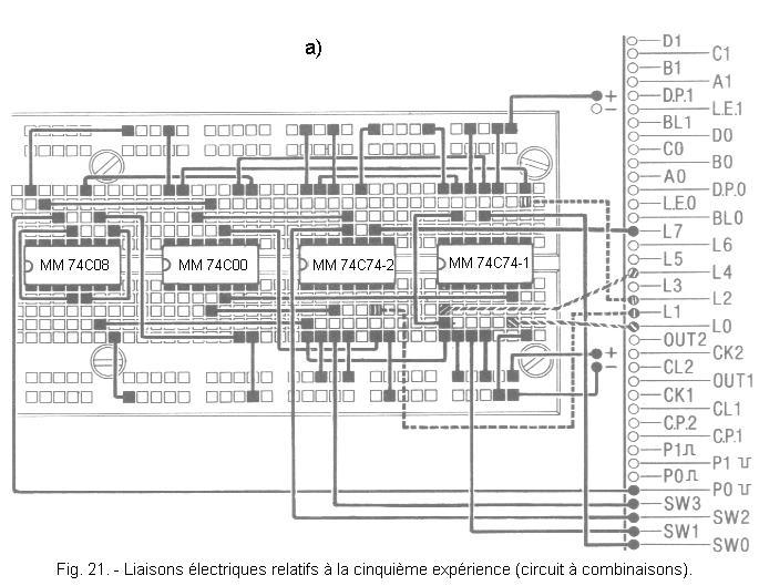
b) Take two integrated circuits MM 74C74 (double D flip-flop), one MM 74C00 (quad NAND) and one MM 74C08 (quadruple AND) and insert these circuits on the matrix as shown in Figure 21-a.
c) Make the connections indicated in Figure 21-a omitting for the moment those traced in dotted line.
d) Set the switches to the 0 position.
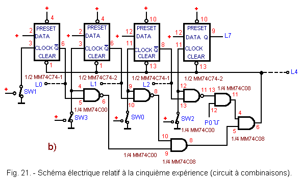
The realized circuit is shown schematically in Figure 21-b. It can appear complex but in fact, it is quite simple. The two circuits MM 74C74 are differentiated ; one is noted MM 74C74-1, the other MM 74C74-2.
The PRESET inputs of the four flip-flops are wired at the positive voltage, therefore inactive.
The DATA inputs are wired in the same way to the positive voltage ; the CLOCK inputs are connected to the switches as follows :
first toggle circuit MM 74C74-1 to SW1
first toggle circuit MM 74C74-2 to SW3
second flip-flop of the circuit MM 74C74-1 to SW0
second flip-flop of the circuit MM 74C74-2 to SW2
By putting a switch in position 1, a positive transition is applied to the CLOCK input of the flip-flop and the DATA input is transferred to the Q output. Q goes to the H level,
to the L level.
A network consisting of three NAND circuits and three AND circuits is connected to the three switches SW3, SW0, SW2 and to the three outputs of the first three flip-flops. The network output signal controls the CLEAR inputs of the four flip-flops.
During the manipulation, you will study the function of this network.
The output signal of the circuit is the Q output of the fourth flip-flop and controls the LED L7.
8. 2. - CONTROL OF OPERATION
a) Connect the power supply : LED L7 is off. Otherwise, press P0 to turn L7 off. This gives you the desired initial conditions.
b) Set the switches to position 1 in the following order : SW0, SW1, SW2, SW3 : the situation is unchanged, LED L7 remains off.
c) Return the switches to position 0, then reposition them at level 1 in the following order : SW1, SW3, SW0, SW2. LED L7 lights up.
d) Return the switches to position 0 :L7 remains lit.
e) Press P0 : L7 goes off, you are in the desired initial conditions.
f) Do several tests by successively positioning the four switches on 1 in any order. Only the sequence SW1, SW3, SW0, SW2 makes it possible to switch on L7.
In conclusion, this logic circuit recognizes a single combination among the 24 possible combinations with four switches.
g) Disconnect the power supply.
IMPORTANT NOTE :
If the circuit does not work as expected, carefully check the connections made and make sure that the conductors are firmly seated in the different contacts of the matrix and the connector group. Also check the insertion of the integrated circuits in the matrix, at their orientation and their pins.
In the event of failure, you may suspect a defective integrated circuit. In this case, check the individual operation of each integrated circuit using the different study assemblies previously made for each type of integrated circuit.
a) Connect the power supply, set the four switches to the 0 position and press P0 ; you observe this :
L0
is lit, so the output of the first flip-flop is at level H
L1
is lit, so the output of the second flip-flop is at level H
L2
is lit, so the output of the third flip-flop is at level H
L4
is lit, the CLEAR des quatre
input of the four flip-flops is at level H.
Under these initial conditions, the four flip-flops are in state 0, ready to receive the correct sequence of the four switches.
b) Now put SW1 on position 1. The LED L0 goes out, the first rocker has transferred a level H at output Q and is at level L.
c) Set the other three switches to position 1 in order SW3, SW0, SW2. LEDs L1, L2 go out and finally L7 turns on. By setting SW3 and SW0, the second and third flip-flops are switched to the H level and the
outputs are switched to the L level. The action on SW2 transfers an H level to the Q output, L7 lights up.
The exact sequence is thus confirmed by the successive extinction of L0, L1, L2 and the ignition of L7 and L4.
d) Return the four switches to the 0 position and press P0.
You notice that L4 goes out, a level L applied on the CLEAR inputs resets the four flip-flops (LED L0, L1, L2 on, L7 off).
Here is what happens when the order is not respected.
e) Set SW1 to position 1 :LED L0 goes out.
f) Now put SW0 on position 1 instead of SW3.
LED L4 goes out, the four flip-flops are reset by the CLEAR inputs. The circuit is blocked and by activating the other switches, SW3 and SW2, there is no possibility of unblocking the circuit. This result is obtained with the NAND and AND network which has an L level at the output and forces the latches to state 0.
In conclusion, the operation of the circuit can be summarized as follows :
by setting the four switches to the 0 position and pressing P0, the circuit is predisposed for operation.
by actuating the four switches in the determined sequence (SW1, SW3, SW0, SW2), the circuit enables the lighting of the LED L7.
any other sequence is not recognized by the circuit and the LED indicator L7 remains off.
In addition, by changing the designations of the four switches, you can change the combination. It is also possible to increase the number of switches by adding a flip-flop for a new switch. It is necessary to add NAND and AND circuits and the overall circuit becomes more complex.
This circuit illustrates in the most complete way the concept of memory circuit. A circuit consisting solely of logic gates can not recognize a sequence, but a latch circuit is able to remember past events.
The case examined is particularly clear : each latch memorizes an event, constituted by the closing of the corresponding switch.
Note that the dotted lines are used to visualize the voltages at certain points of the circuit and do not play any role in the operation of the circuit.
You will always be able to establish this type of connection to help you understand a circuit.
In the next practice, you will discuss the monostable exam.


 Realization of a circuit with combinations
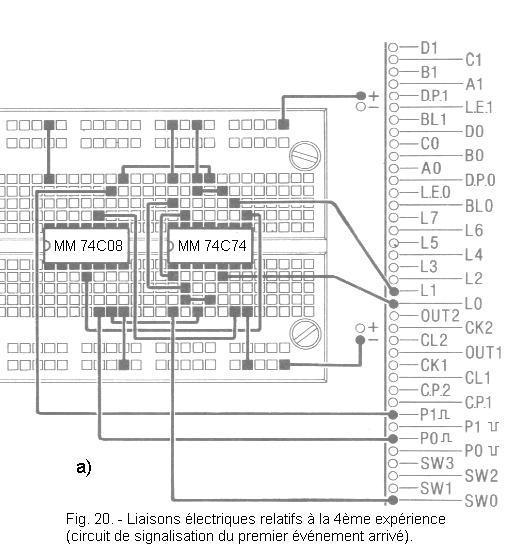
 Click here for the next lesson or in the summary provided for this purpose.
 Top of page
 Next Page