D flip-flop in Master-Slave Configuration, JK flip-flop :
5. - SECOND EXPERIENCE : "EXAMINATION OF A ROCKET D IN MASTER-SLAVE CONFIGURATION"
With this manipulation, you will check the operation of a D flip-flop in the master-slave configuration. In a previous experiment, you have already had the opportunity to examine the integrated circuit MM 74C74 containing two D flip-flops; you will learn more about how this circuit works by bringing together some of the points gained from previous experiences.
5. 1. - REALIZATION OF THE CIRCUIT
a) Disconnect the power supply and remove the integrated circuit from the matrix, remove from the group of connectors all the links relating to the last experiment.
b) Insert on the matrix two MM 74C00 integrated circuits (containing four NAND circuits each) and one integrated circuit MM 74C04 (containing six inverters) in the positions shown in Figure 16-a.
c) Make the connections described in Figure 16-a using as usual insulated tin wire recovered from previous experiments or cut to the proper length in the strand you have in your possession.
d) Set the SW0 switch to the 0 position.
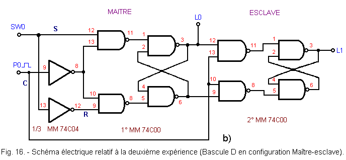
The wiring diagram of the circuit you have just made is shown in Figure 16-b. As you can observe, the circuit consists of two R.S.C flip-flops of the type that you have already examined in the previous practice, connected one after the other.
The
signal provided by the P0 button is applied directly to the input of the second flip-flop and through an inverter at the input of the first.
A second inverter, connected to the input R of the first flip-flop, makes it possible to invert the logic levels applied to the inputs S and R by means of the switch SW0.
Note that the first flip-flop is called Master while the second is called Slave. These terms were chosen to highlight the fact that the second flip-flop is slaved to the first as you will see in this manipulation.
5. 2. - OPERATING TEST
a) Connect the power supply. You observe that the LED L0 connected to the output of the MASTER rocker is off, indicating that this output is in state L.
The LED L1 connected to the output of the SLAVE toggle is either on or off, depending on the state of the circuit at power up. This is not predictable and depends on the physical characteristics of the integrated circuit.
b) Switch the SW0 switch several times. You notice that the output of the MASTER latch follows the state of the input, going to state H (L0 on) or state L (L0 off) when the switch SW0 is switched respectively to the position 1 (circuit input in the H state) or 0 position (circuit input in the L state).
On the other hand, the LED L1 does not signal any change of state at the output of the SLAVE rocker.
With this test, you have made sure that the MASTER flip-flop is sensitive to the level of the input signal when the input C of the circuit is in the L state, while the SLAVE flip-flop is insensitive.
c) Now turn switch SW0 to position 1 so that L0 is lit.
d) Press the P0 button and hold it in this position, thus applying a level H to the control input C of the circuit.
You observe that L1 turns on or stays on if it already is ; this indicates that the output status of the MASTER has shifted to the SLAVE output.
e) Keeping P0 still pressed, switch the SW0 switch several times.
You observe that L0 remains lit, a sign that the MASTER does not change state and is therefore insensitive to variations in the level of the input. Similarly, by observing L1, you find that the SLAVE, too, does not change state.
f) Release the P0 button and switch the SW0 switches repeatedly.
This time, you notice that L0 turns on and off each time you act on SW0. This indicates that the output of the MASTER is again following the level changes of the input. On the other hand, L1 remains constantly lit indicating that the exit of the SLAVE does not change state.
g) Set switch SW0 to position 0 so that L0 goes out.
h) Press and hold P0 in this position ; L1 goes out.
i) Release the P0 button : L1 remains off.
With this test, you have practically verified the operation of the MASTER-SLAVE circuit which can be summarized as follows :
when the control input C is in the L state, the MASTER outputs the logic state present on the input. The SLAVE is however isolated from the MASTER and is therefore insensitive to any variation of state manifesting itself on the input.
When the control input C goes to state H, the MASTER is isolated from the input and its output becomes independent of the state of the input, and the state present at the output of the MASTER is transferred to the exit of the SLAVE.
We can therefore conclude that in a MASTER-SLAVE type flip-flop the transfer of the logic states of the input terminals to the output terminals is done in two stages : the time to perform this transfer is equal to the duration of a pulse of clock (which can be of the order of 1 µs or even less in commonly used circuits).
When the clock pulse (input C) goes from H to L, the data present at the input is transferred to the MASTER (and there is no change at the output of the flip-flop, that is, say SLAVE).
At the moment of the transition from L to H of the clock pulse, the data present at the output of the MASTER is transferred to the SLAVE, therefore to the output of the flip-flop.
J.K. Master-Slave, as you will see in this manipulation, is the most versatile type of job switch you will have to examine.
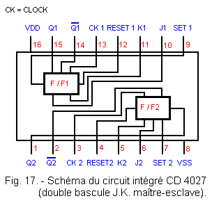
For this manipulation, you will use the integrated circuit CD 4027 (or equivalent type) containing two flip-flops J.K. MASTER SLAVE whose inputs and outputs are connected to the pins according to the diagram of Figure 17.
The two flip-flops are identical and as you can see, each of these flip-flops has five inputs.
two main entrances J and K
CLOCK clock input
two auxiliary inputs SET and RESET
The functions of these entries will be verified directly by the following manipulation.
The outputs of each flip-flop are two in number, Q and ,
and they are complementary to each other.
6. 1. - REALIZATION OF THE CIRCUIT
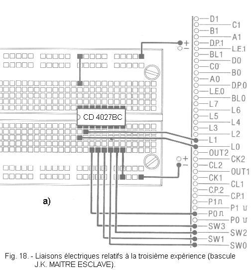
a) Disconnect the power supply and remove from the matrix and the connector group all the integrated circuits and connections related to the previous experiment.
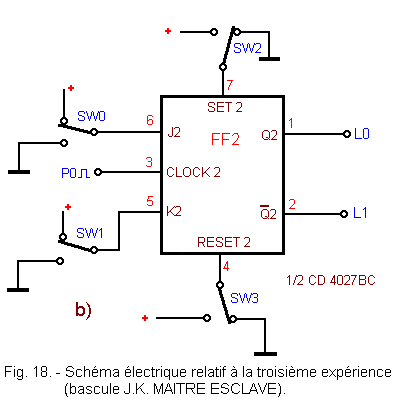
b) Insert the circuit CD 4027 on the matrix in the position indicated in Figure 18-a, and make the connections reported in this same figure.
The circuit diagram of the realized circuit is shown in Figure 18-b. As you can see, inputs J2 and K2 are respectively connected to SW0 and SW1, while inputs SET 2 and RESET 2 are connected to SW2 and SW3.
Outputs Q2 and 2
are connected to LEDs L0 and L1.
Since, as we have already said, the two flip-flops constituting the integrated circuit are perfectly identical, the operating test is limited to only one of them, so all the pins from the 9th to the 15th are left free.
6. 2. - OPERATING CONTROL
a) Power the circuit : one of the two LEDs L0 and L1 lights up. It is not possible to predict which of the two will light, because it depends on the physical characteristics of the integrated circuit.
b) Switch switch SW2 to position 1 thus setting SET 2 to H. The LED L0 connected to output Q2 lights up or stays on.
c)Put switch SW2 back to position 0 and switch switch SW3 to position 1, thus applying state H to input RESET 2.
You observe that the LED L0 goes out, while the LED L1 connected to the output 2 comes on.
d) Switch switches SW2 and SW3 several times, taking care, however, never to put them both in position 1. You notice that each time switch SW2 is in position 1 (SET 2 on level H), output Q2 also goes to level H, while 2
goes to level L.
On the other hand, when SW3 is on position 1 (RESET 2 on level H), the output Q2 passes on level L and 2
au niveau H.
e) Set SW2 to position 1 (SET 2 to state H) and SW3 to position 0 (RESET 2 to state L) so that L0 lights, then operate as many times as you want switches SW0 (input J2), SW1 (input K2) and the button P0 (input CLOCK 2).
You notice that the state of the outputs Q2 and 2
does not vary, which indicates that the changes of state of the inputs J, K and CLOCK do not determine any switching of the state of the outputs.
f) After switching SW2 to position 0 (SET 2 to state L) and SW3 to position 1 (RESET 2 to state H) for L1 to turn on, redo the previous test by operating several times SW0, SW1 and P0.
You observe that in this case also, the inputs J, K and CLOCK do not cause a change in the state of the outputs.
With these tests, you could see that the SET and RESET inputs force the flip-flop in one of its two possible states, independently of the other inputs.
g) Set both switches SW2 and SW3 to position 1. In this case both LEDs L0 and L1 light up ;however, this condition is generally neither useful nor advisable.
h) Simultaneously switch SW2 and SW3 to position 0. The flip-flop will go to a state that will depend on which one of the two inputs SET and RESET remains last on position 1.
i) Set the scale to 0 so that L0 is off and L1 is on. Put SW3 for a moment on position 1 then put it back on position 0.
j) Leaving SW2 and SW3 on position 0, also SW0 and SW1 switch to position 0, so you apply state L to both inputs J2 and K2. Then press and release the P0 button. You observe that the scale remains in state 0 (LED L0 off).
k) Set SW0 to position 1 (J2 to H), leave SW1 to position 0 (K2 to L) and press the P0 button. You observe that L0 lights up, while L1 goes out
l) Release P0 : L0 remains lit.
m) Set SW0 to position 0 (J2 to state L) and SW1 to position 1 (K2 to state H). Press and release the P0 button. You notice that L0 goes off while L1 turns on.
n) Now switch SW0 to position 1 ; in this way J2 and K2 are at level H.
o) Press P0 : L0 lights up and L1 goes out.
p) Release and then press again P0 : L0 goes off and L1 lights up.
By continuing to press and release P0, you will see a change of state every time. It can thus be concluded that when the inputs J and K are both at the level H, the flip-flop changes state each time a positive pulse occurs on the CLOCK input, that is to say whenever there is a transition from level L to level H.
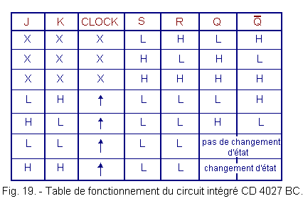
The results of the tests carried out are shown in Figure 19, in which the operating table of the rocker in question is reported.
Remember that in this table the symbol X means "indifferent state" while the arrow with the tip pointing up represents a transition of the clock signal from level L to level H. The letters S and R respectively indicate the SET and RESET inputs.
In conclusion, the operation of the J.K. MASTER-SLAVE rocker can be summarized as follows :
the two inputs SET and RESET must be at the level L to obtain the normal operation of the flip-flop with the clock signal.
if the J input and the K input are both in the L state, there will be no change of state at the output when a positive transition occurs on the CLOCK input.
if input J is in state H and input K is in state L, the flip-flop goes (or remains if it is already there) to state 1 (output Q at level H and output at level L) when a positive transition is applied to the CLOCK input.
if the input J is in the state L and the input K in the state H, the rocker passes (or remains if it is already there) in the state 0 (exit Q at the level L and exit at the level H) when a positive transition is applied to the CLOCK input.
if the J input and the K input are both in the H state, the flip-flop changes state each time a positive level transition is applied to the CLOCK input. In this case, it is said that the flip-flop operates in T (toggle) mode. This mode of operation is the basis of many types of electronic counting systems as you will see later.
if the SET input is at the H level and the RESET input at the L level, the flip-flop immediately goes to the 1 state (Q at the H level and at the L level) without the need for a positive clock pulse.
if the RESET input is at the H level and the SET input at the L level, the flip-flop immediately goes to the 0 state (Q at the L level and at the H level) without the need for a positive clock pulse.
if the SET and RESET inputs are both at the H level, both Q and outputs immediately go to state 1. However, this condition must be avoided.
for normal operation of the flip-flop, the clock signal must be free of noise and characterized by a transition time from level L to level H less than 5 µs, for example that obtained by acting on the button P0 (P0 contact
on the connector group).
The operation described above, relative to the integrated circuit examined, is also that of any JK type flip-flop.
However, the SET and RESET inputs instead of being active at the H level may be at the L level. This means that these two inputs must be held at H level for a flip-flop operation with the clock signal.
On the other hand, when one wishes to position the rocker independently of the clock signal, the input SET or the entry RESET must be brought to the level L.
In this case, a small circle (inversion sign) is placed on the two SET and RESET inputs in the diagram representing the flip-flop
There are also latches requiring a negative clock transition, that is to say a signal from level H to level L.
In this case too, a small circle is reported on the CLOCK input terminal in the diagram ; it indicates that the CLOCK input is active with a negative transition of the clock signal.
The J.K. flip-flop is certainly more versatile than the D flip-flop and has some characteristics with respect to the latter, which make it irreplaceable in certain applications. In other cases, the flip-flop D is often preferred because having a single input D, its use reduces the complexity of the systems. In addition, this D flip-flop has the advantage of being a little more economical and consuming less energy than the J.K flip-flop.


 Examination of a rocker JK
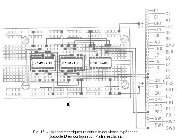
 Click here for the next lesson or in the summary provided for this purpose.
 Top of page
 Next Page