Study of the Series Offset Circuit - Parallel "MM 74C175" :
5. - FIRST EXPERIENCE : OPERATING TEST OF A SERIES - PARALLEL SHIFT CIRCUIT
A shift circuit is constituted by a fixed number of flip-flops interconnected in cascade. At each clock edge, the data transits from one flip-flop to the next.
On the market, there are shift registers in the form of integrated circuits.
In this experiment, you will realize a shift circuit with four elementary latches in order to understand the operating principle. These four D-type synchronous flip-flops are contained in the integrated circuit MM 74C175 described in the previous practice.
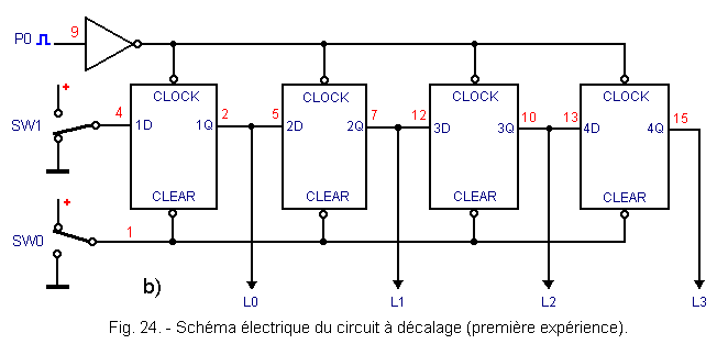
The Figure 23 shows the circuit diagram of the MM 74C175 circuit. The four CLOCK inputs are connected together. The same goes for the four CLEAR entries.
The CLOCK input is active at the rising edge of the clock, while the CLEAR input is active at a logic level L.
With this experiment, you will connect these four latches to form a series-parallel register.
5. 1. - REALIZATION OF THE CIRCUIT
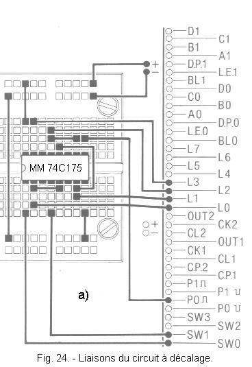
Insert the MM 74C175IC into the array and make the connections shown in Figure 24-a.
Figure 24-b shows the circuit diagram of the assembly. It is the switch SW1 connected to the input D of the first flip-flop which allows you to choose the logical data to be transferred into the register. You notice that the output Q of this first flip-flop is connected to the input D of the second and so on.
The four LEDs show the logical state of the four flip-flop outputs. The pushbutton P0 provides the clock signal.
5. 2. - OPERATING TESTS
a) Make sure the digilab power switch is in the "OFF" position, that is, the power is off and insert the plug into the 220 volt outlet.
b) Put SW0 on position 0 and SW1 on position 1.
c) Turn on the power by switching the switch to the opposite position from "OFF". The four LEDs are off, all four CLEAR inputs are active.
d) Set SW0 to position 1. Thus CLEAR inputs are inactive.
e) Press and release the P0 button : LED L0 lights up. Indeed, the data present on the input 1D is transferred to the output 1Q at the clock edge. It is also found on the 2D input of the second flip-flop.
f) Set SW1 to the 0 position.
g) Press and release P0 : LED L0 goes out and LED L1 lights up. Indeed, the data 1D is transferred to the output 1Q, so L0 goes off ; and the 2D data is transferred to the output 2Q, hence the ignition of L1.
h) Press and release P0 : LED L1 goes out and LED L2 lights up.
i) Press P0 again : LED L2 goes out and LED L3 lights up.
j) By pressing P0 one last time, you observe that L3 also goes out.
This shows that the data (state 0) initially present in 1D is transferred from one flip-flop to the next at each active clock edge. This is indicated by the extinction of the various LEDs.
In this arrangement, four clock periods are necessary for the data initially located in 1D to be transferred to the output 4Q.
At the fifth clock face, the data disappears since there are only four flip-flops.
k) Put SW1 on position 1.
l) Press P0. LED L0 lights up.
m) Press P0 again. LED L1 lights up and L0 stays on.
n) Press P0 again twice. LED L2 lights up, then LED L3. At this point all four LEDs are lit.
Indeed, at each clock edge, there is a shift of data from one flip-flop to the next. In our case, the data is permanently 1.
o) Return SW1 to the 0 position and press P0. LED L0 goes out. Indeed, the data has just been transferred to the output 1Q of the first flip-flop.
p) Return SW1 to position 1 and press P0. LED L0 lights up again, L1 goes out and L2 and L3 stay on.
q) If you press P0 repeatedly, you observe that the LED that is off shifts from one position to each clock edge. After the binary 0 data transfer at 4Q output, if you press again, you will see that the four LEDs remain lit.
At first, you observed the shift of a lit LED then that of an LED off.
r) The experiment is over. Set the digilab switch to "OFF". Disconnect the mains plug.
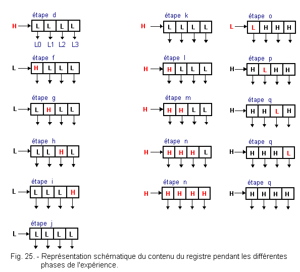
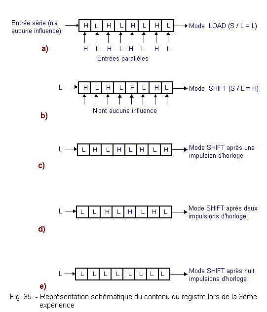
Figure 25 schematically illustrates the evolution of the shift register during the various stages of the experiment. Each square symbolizes a rocker.
The four downward arrows represent the four outputs L0, L1, L2 and L3.
The letter L in a square symbolizes a low logical level on the output of the corresponding flip-flop, the letter H in a square symbolizes a logical high level. The arrow to the left of the four squares represents the 1D serial input. The transition from one state to another of the register occurs at each clock pulse on the CLOCK input.
In this Figure 25, the steps d to j show the shift of a logic data item at the level H.
From step k to step n, you attend the total loading of the register with logical data at level H.
From step o to step q, it is the shift of a logic data item at the level L.
In conclusion, the operation of a series-parallel shift register can be summarized as follows :
at each active edge of the clock, the data present in 1D is transferred to the first stage of the register.
simultaneously each bit of information transits from one floor to the next. The information bit of the last flip-flop is lost.
Each stage of the register has an output. Also remember that there are serial-series registers. These only have one serial output. This is the one that corresponds to the exit of the last floor of the examined installation.
These series-series registers are used when the intermediate outputs of each stage are not necessary or when the register consists of a too high number of stages.
6. - SECOND EXPERIENCE : EXAMINATION OF THE INTEGRATED CIRCUIT MM 74C164
The MM 74C164 is an eight stages series-parallel shift register.
In this manipulation, you will check its operating characteristics so that you can use it later in future experiments.
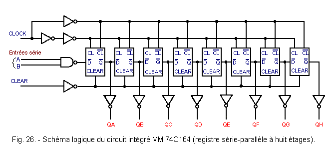
The Figure 26 shows the logic diagram of this circuit.
It consists of eight D type flip-flops connected in cascade. The
output of each flip-flop is connected to the input of the next flip-flop.
CLEAR input is common to all scales. It is active at the L level and forces the Q outputs of the latches to logic 0.
The CLOCK input is also common to all flip-flops. It is active on the rising edge of the clock.
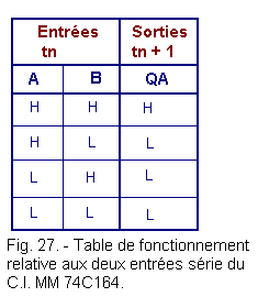
There are two serial inputs A and B. The operation of these is defined by the operating table located in Figure 27.
The instant tn is the instant that precedes the active clock edge. The instant tn + 1 is the one that follows the active clock edge.
It appears that if A and B are at level H at time tn, output QA will be at level H at time tn + 1.
In all other cases, it suffices that only one input is at the logic level L so that the output QA goes to the level L at the active clock edge.
This operating table is therefore analogous to that of an AND circuit.
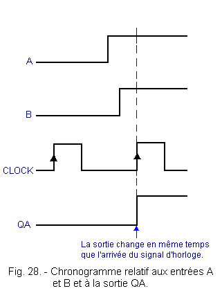
In Figure 28, you notice that the QA output goes to the H level simultaneously to the active edge of the clock since the two inputs A and B are previously brought to the H level.
The integrated circuit MM 74C164 works in the same way as the assembly of the first experiment.
That is to say that at each clock pulse the data present in QA is shifted in QB, that of QB in QC, etc ...
The data present in QH is lost at each new pulse.
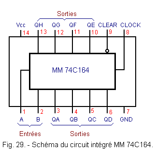
Figure 29 shows the circuit diagram and pinout of the integrated circuit MM 74C164.
6. 1. - REALIZATION OF THE CIRCUIT
a) Remove from the matrix the connections relating to the previous experiment, as well as the integrated circuit MM 74C175.
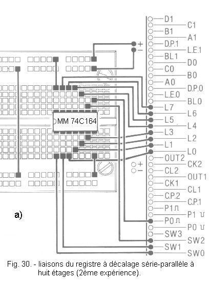
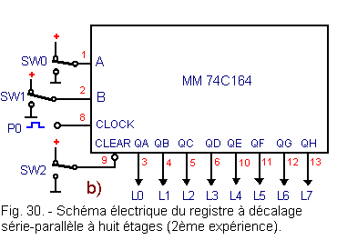
b) Insert the integrated circuit MM 74C164 on the matrix and make the connections indicated in Figure 30-a.
Figure 30-b shows the circuit diagram of the realized circuit. The integrated circuit is represented by the rectangle.
The eight outputs are connected to the eight LEDs. Inputs A and B are wired on switches SW0 and SW1. The CLEAR input is controlled by switch SW2. The clock signal is provided by P0.
6. 2. - OPERATING TEST
a) Plug in the mains plug. Set SW2 to 0. Then turn on the power. All LEDs are off.
b) Set SW2 to position 1. The register is ready for operation.
Check circuit operation by trying all possible combinations on inputs A and B.
c) First put SW0 and SW1 on position 1 and press P0 :LED L0 lights up.
d) Set SW1 to 0 and press P0 : LED L0 goes out and L1 lights up.
e) Press P0 repeatedly. You observe that the lit LED shifts each time one floor. By pressing one last time when the LED L7 is lit, you will find the initial position, that is to say the eight LEDs off.
f) Switch SW0 to position 0 or position 1 and press P0 each time. The LEDs remain off.
You have checked that if the input B is at the level L, the register is invalid and can not take into account the logical data present on the entry A. This entry B can thus be used as validation input.
g) Reset SW0 and SW1 to position 1. Press P0 repeatedly. At each active clock edge, you turn on one more LED. Each bit of information transits from one floor to the next.
h) Put SW0 on the 0 position. Repeat the same experiment as in f). You reverse the role of SW0 and SW1. This time it is the entry A which invalidates the register. A has become an order entry.
Thus, you can use as input validation, the entry of your choice.
When this test is complete, set the digilab switch to "OFF" and unplug the mains plug.
7. - THIRD EXPERIMENT : INTEGRATED CIRCUIT OPERATING TEST MM 74C165
In both previous experiments, you have examined the operation of serial-parallel shift registers with serial input and parallel outputs. As you could see, the logical data were applied one after the other at the serial input (that is why the register works in serial mode) and then presented simultaneously on the outputs (parallel mode).
Conversely, there is another type of shift register that you will examine. In the latter, it is possible to enter the data simultaneously in all the stages of the register, then to shift to a single output the data thus recorded. This operating mode is called "parallel input and serial output".
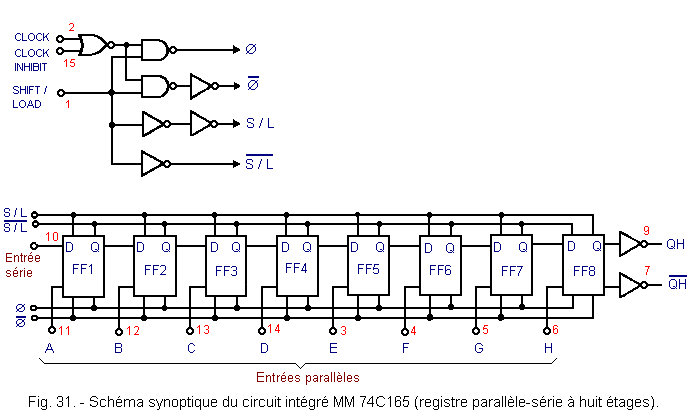
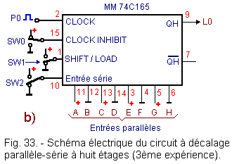
In Figure 31 is shown the block diagram of the integrated circuit MM 74C165 (eight stages shift register) that you will use in this manipulation.
The eight stages, consisting of eight flip-flops, are connected one after the other, as in the shift register examined previously.
Note, however, the presence of eight entries rated A to H, each of which is connected to a rocker. These inputs are parallel inputs.
The first flip-flop FF1 has, in addition, an input called serial input, similar to that of the registers examined in the two previous experiments.
So this register can work either with a serial input, that is to say in the way you already know, or with parallel inputs, as you will verify in this experiment.
Since these two modes of operation are mutually exclusive, there is a command entry called SHIFT / LOAD that allows you to switch from one to the other.
When the SHIFT / LOAD input is at L level, the register loads with parallel inputs (LOAD mode) ; when it is at level H, the circuit operates as a serial input register. The data present on this serial input is transferred to the output of the first flip-flop at the first clock pulse. It shifts in the register at each of the following clock pulses (SHIFT mode).
Finally, the data present on the serial input are found one after the other on the single output QH.
Also observe that the circuit has two different CLOCK inputs : one specifically called CLOCK is the one usually used as clock input ; the other called CLOCK INHIBIT (that is, clock inhibition) works as a control input. If it is at level H, the CLOCK input is disabled or inhibited, which means that the latter is no longer active.
Note however, that the CLOCK and CLOCK INHIBIT inputs terminate at the same NOR gate
(pin 2 and pin 15 in Figure 31). Thus, their roles can be interchanged. Thus, it is possible to use terminal 2 as control input (clock inhibition) and terminal 15 as input of the clock signal.
The NAND, NOR and INVERSE gate array shown at the top of Figure 31 serves to provide, from the two CLOCK inputs and the SHIFT / LOAD input, the control signals for the eight flip-flops.
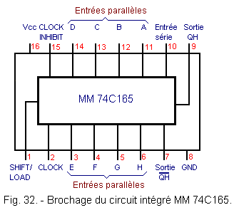
Figure 32 shows the pinout of the integrated circuit examined.
7. 1. - REALIZATION OF THE CIRCUIT
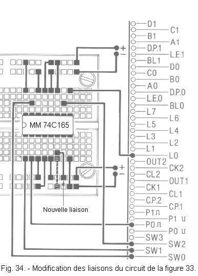
a) Remove all links relating to the previous experiment and remove the integrated circuit MM 74C164 from the matrix.
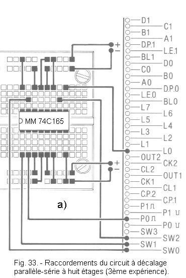
b) Insert the integrated circuit MM 74C165 on the matrix and make the connections indicated in Figure 33-a.
Figure 33-b shows the wiring diagram of the circuit you made ; the register is schematically represented by a rectangle from which the terminals relating to the inputs and outputs of the circuit start.
As you can see, the parallel inputs are alternately connected to positive voltage and ground. The serial input is, on the other hand, connected to the inverter SW2 and can thus be brought to the level L or H.
On the input CLOCK is applied the signal of the contact P0.
The CLOCK INHIBIT input is controlled by SW0, the SHIFT / LOAD input by SW1.
The state of the QH output is visualized by the LED L0.
7. 2. - OPERATING TEST
a) Place SW0 on position 1, SW1 and SW2 on position 0. Then insert the plug in the socket and turn on the digilab, you observe that LED L0 is off.
Indeed, the input SHIFT / LOAD being at level L, the integrated circuit operates in LOAD mode and each latch is carried to the logical level present on its parallel input. Now, the H input is L level, so the QH output is also at the L level and the L0 LED is off.
The state of the other flip-flops can not be known because their outputs do not lead to any pin of the integrated circuit. Nevertheless, it will be possible to know these states indirectly.
b) Remove the link between pin 6 of the integrated circuit and the ground (in dotted line in Figure 34) and put it between pin 6 and the positive supply line, as shown in this same Figure 34.
You observe that L0 lights up. Indeed, with this new connection, the input of the eighth rocker (pin 6) is at the level H. So the output of this same rocker goes to the same level H.
c) Restore the previous link (between pin 6 and earth) : LED L0 goes out again.
In the same way, even if it is not possible to check it, the logic level of the outputs of the other flip-flops is the same as that present on the inputs.
d) Set SW1 to position 1 : in this way, the operation of the integrated circuit changes from LOAD mode to SHIFT mode. The register then retains the eight logical states present on the eight parallel inputs. If the logical data present on these eight inputs change, they will not be taken into account by the register which is now switched to serial-serial mode.
e) Check this by repeating the previous test. To do this, temporarily disconnect pin 6 from the ground and connect it to the positive voltage line. You notice that L0 remains off.
To verify the correct loading of the register with the eight logical data, you will perform a series-series shift. Thus, you will collect QH output these eight logical states one after the other.
f) Put SW0 on position 0. You thus validate the clock input. Using P0, send a positive impulse: you see that L0 lights up. Indeed, during the rising edge applied to the CLOCK input, the content of the seventh latch (logic level H) was transferred to the eighth latch, so at its output QH.
g) If you continue to send pulses using P0, you notice that L0 turns on and off alternately, since the register has been loaded, in alternating order, by a level H and a level L.
After the first eight pulses, it only appears logical levels L output QH. Indeed, SW2 is on position 0 and from the first pulse, it is a level L which is loaded in the first stage. At each subsequent pulse, the level L is shifted.
If the serial input was at level H, after eight clock pulses, it would have been found that the register is fully loaded with levels H.
h) Continue the test by setting switch SW2 to position 1. You notice that it takes eight clock pulses, that is to say eight successive presses on P0, so that the logical level applied to the serial input by SW2 is transferred to QH output.
i) Now set switch SW0 to position 1 and press P0 : the output of the register does not change state and the LED L0 remains on or off according to the state where it was previously.
Under these conditions, the inhibition input of the clock is active and the clock signal can not change the state of the different outputs.
j) Turn off the digilab and remove the plug from the power outlet.
As you have noticed, the integrated circuit MM 74C165 examined has two modes of operation. Depending on the logic level present on the SHIFT / LOAD command input, it can operate as a parallel-series or serial-series shift register.
In summary, its characteristics are as follows :
When the SHIFT / LOAD input is at the L level, the circuit operates in parallel-serial mode and the contents of the register reflect the logic states present on the parallel inputs, as shown schematically in Figure 35-a. The serial input has no influence on the contents of the register.
When the SHIFT / LOAD input is at the H level, the circuit operates as a serial-series register (Figure 35-b) and each clock pulse shifts the contents of the register by one position. The parallel inputs have no influence on the operation of the circuit and the information present on the serial input is shifted as and when in the register (Figure 35-c, Figure 35-d and Figure 35-e).
If the CLOCK INHIBIT input is raised to H, the CLOCK input is no longer active.


 MM 74C164 Integrated Circuit Review
.gif)
 Click here for the next lesson or in the summary provided for this purpose.
 Top of page
 Next Page