4. - LOGICAL FUNCTIONS WITH BIPOLAR "TTL" TRANSISTORS
As an introduction to the TTL (Transistor - Transistor - Logic), we will return to the DTL with Figure 20.
We see a great similarity between the input circuit of an operator in DTL technology and the symbol of the transistor (symbol very little used, but which well image the two junctions of which it is constituted).
To obtain several inputs, simply add several diodes on the transmitter side. We come to the multi-transmitter transistor, which is found in almost all TTL operators.
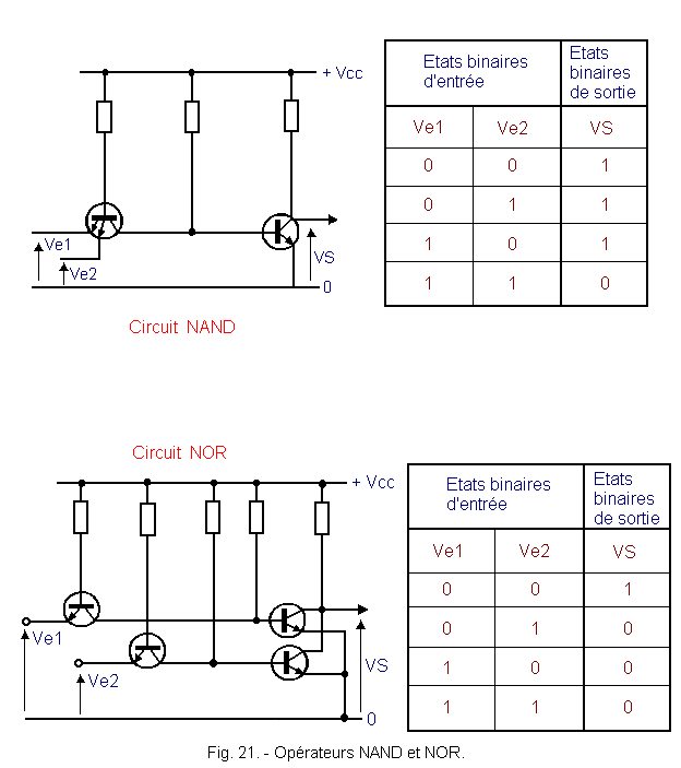
In this technology, Figure 21 represents the NAND and NOR operators as well as the truth tables.
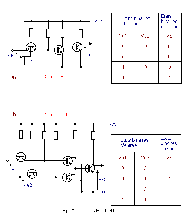
Figure 22 shows the previous circuits, NAND and NOR, to which are added NON circuits in order to obtain the AND and the OR with the related truth tables.
Some modifications have been made to these operators for the sake of improvement.
We will examine them below.
Improvements over the basic assembly.
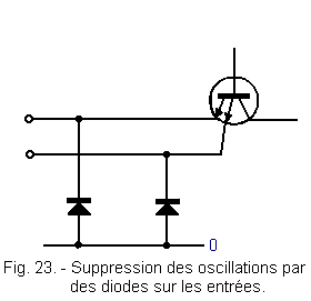
One of the characteristics of this technology is to switch quickly, that is to say to move very quickly from one state to another. This is an advantage, but in these very short times, the wiring and connections represent chokes and capacitors that oscillate in the presence of these signals.
These damped oscillations are recorded by the following operator as a series of states and states 1.
To overcome this disadvantage, a diode is placed on each input as shown in Figure 23.
On the other hand, these operators using a transistor mounted as a common emitter, have a "resistance" output too high compared to the "resistance" input operators they are likely to control.
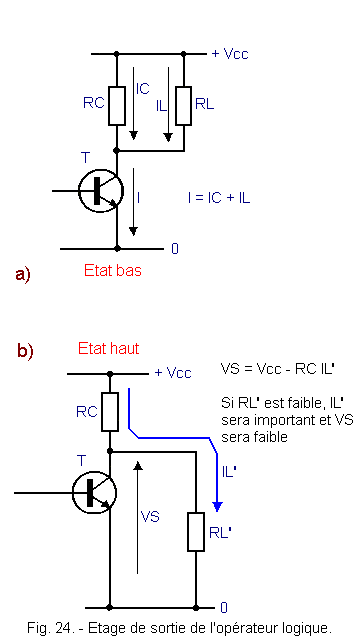
Figure 24 represents the output stage of an operator to which a load constituted by the inputs of other operators has been connected.
This load is different depending on the output state of T (state 1 or high and state 0 or low).
At the low level, the input transistors of the following stages are conductive and the current IL is important.
At high level, these same transistors are blocked, there is nevertheless a current IL' (due among other things to the reverse currents of the diode junctions of which we spoke previously).
At the low level, the transistor T will have to support its own collector current plus the emitter current of the following operators.
One is tempted to say that it would suffice to reduce as much as possible its own collector current to mitigate this phenomenon by increasing RC.
Now, if we increase RC, at the high level, the inverse currents of the junctions walk as shown in Figure 24-b and we see that if RC increases and RL' decreases, the high level VS becomes so low that there will be little difference between high and low levels.
You can see that the currents IL and IL' are in opposite directions. We'll talk about it again later.
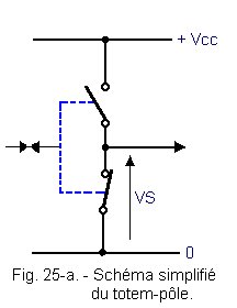
It is therefore necessary to abandon this arrangement in favor of another whose output resistance will be lower. This new montage is called : "Totem pole".
Figure 25-a is a simplified representation of this arrangement which can be likened to two switches, one being open, the other closed and vice versa, both can not be opened or closed at the same time.
We can already understand the interest of this montage.
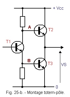
The two switches are actually transistors, as shown in Figure 25-b, connected in series and controlled in opposition, that is to say that one imposes the saturation of one and the blocking of the other.
In the high state, T1 is saturated and T2 is blocked.
The VS output is at + VCC potential.
In the low state, T1 is blocked and T2 is saturated.
Output VS is at potential 0.
In reality, things are not so simple. Let's go back to Figure 25-b and suppose that T1 is saturated.
The potential of point A goes down, that of point B will go up.
The voltage VBE of T3 is reached and this leads.
The voltage VS is equal to VCE SAT of T3.
The voltage at B is equal to VBE of T3.
The voltage at A is equal to the voltage at B plus the voltage VCE SAT of T1.
VS = VCE
SAT (T3) -------------->
voltage on the transmitter of T2
VA = VBE
(T3) + VCE SAT (T1)
hence the tension
VBE
of T2 :
VA - VS =
VBE(T3)+ VCE SAT(T1)- VCE
SAT(T3)
The two VCE SAT cancel each other and the voltage VBE of T2 is equal to the voltage VBE of T3.
T2 also drives, so it should be blocked.
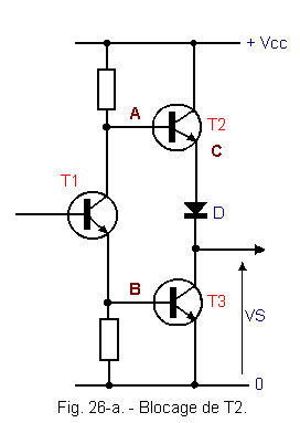
It is therefore necessary to resort to an artifice (that we used previously), by adding a tension equal to this VBE but of opposite sign. For this, we will use the voltage of a junction (diode), polarized in the forward direction. The diagram becomes that of Figure 26-a.
The tensions on this assembly are as follows :
VA = VBE
(T3)
+ VCE SAT (T1)
VB = VBE
(T3)
VC = VCE
SAT (T3)
+ VD
VBE
(T2)
= VA - VC = [VBE (T3)
+ VCE SAT (T1)]
- [VCE SAT (T3)
+ VD]
since :
VBE (T3)
@ VD
VCE
SAT (T1)
@ VCE
SAT (T3)
from where : VBE
(T2) = 0 V.
The transistor T2 is blocked, while T3 is conductive, VS is at potential 0 (low state).
If T1 is blocked, the potential of point B tends to 0 and T3 is blocked.
The potential of A goes back to the + VCC is the voltage VBE of T2 is reached, a current base is established and T2 is saturated.
The potential of VS goes back to + VCC (high state).
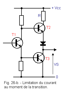
However, there is still a small flaw at the moment of the transition, that is to say before T3 is completely blocked, T2 begins to drive, which results in a current draw that VCC must provide. This current draw will be slowed by the addition of a low value resistor as shown in Figure 26-b.
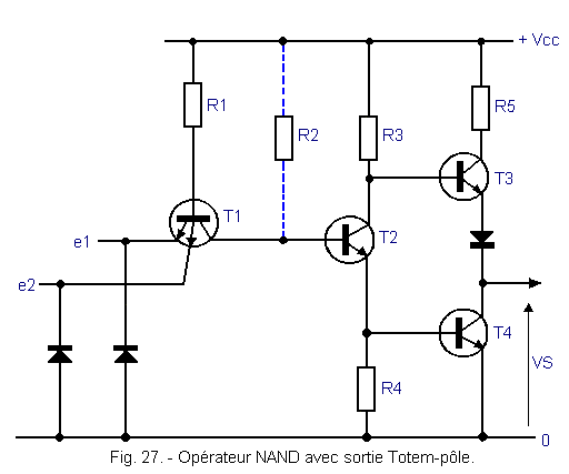
Figure 27 shows a NAND operator as can be found in practice.
In this arrangement, the resistor R2 disappears, the base current of T2 is supplied by the reverse current of the collector-base junction of T1.
As an indication, the following table gives the values of the resistances of this circuit :
R1 = 4 kW
R3 = 1,6 kW
R4 = 1
kW
R5 =
130 W
the supply voltage is
:VCC
= + 5 V
the input current to the high state : 40 µA
the input current at the low state : 1,6 mA
the output current in the high state : 400 µA
the output current at the low state : 16 mA
the output voltage in the high state : 2,4 à 3,4 V
the output voltage at the low state : 0,2 à 0,4 V
the input voltage considered high state : 2 V
the input voltage considered as low state : 0,8 V
These parameters are, in the manufacturer's catalogs, represented by abbreviations. In the next TECHNOLOGY 4 we will list these abbreviations.
From now on, we can talk about it and give some explanations about the TTL.
the supply voltage :
VCC
the input current to the high state :
I IH
I : symbol of the current, the indexIH
correspond to :
I
:
input "entrée"
H :
hight-level "niveau haut"
Low input current :
I IL
The index L
corresponds to : low-level "niveau bas"
the output current in the high state :
I OH
the index
O
corresponds to : output "sortie"
the output current at the low state :
I OL
the output voltage in the high state :V OH
V is the symbol of a tension
the output voltage at the low state :
V OL
the input voltage taken into account as a high level :
V IH
the input voltage taken into account as a low level :
V IL
In logic, it is rare that only one operator is needed to perform a function. It is therefore necessary to associate several of these operators to arrive at the result.
It is therefore advantageous to standardize these inputs and outputs regardless of the operators so as to achieve these associations without stumbling as to the voltage and current levels.
If one uses, in a same assembly, different technologies, for example operators with diodes with TTL, one is led to borrow so-called interface circuits.


 NAND Operator with Totem-Pole Output
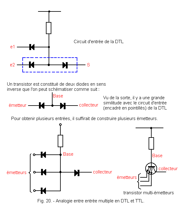
 Click here for the next lesson or in the summary provided for this purpose.
 Top of page
 Next Page