Logic Functions with Diodes - AND - NAND - OR - NOR - NO :
2. - LOGICAL FUNCTIONS IN DIODES
2. 1. - THE FUNCTION "AND" IN DIODES
Figure 8-a shows the AND function with diodes.
The switch i1 sets the input N° 1 to Ve1 = VCC, that is to say to the binary state 1.
The switch i2 sets the input N° 2 to Ve2 = 0, that is to say, the binary state 0.
The output VS, in this case, is at a voltage level equal to the bias of the diode D2 in the forward direction, namely : 0.6 V.
This 0.6 V level will be considered as no voltage, ie the binary state 0.
Binary states :
Ve1 = 1
Ve2 = 0
VS = 0
Figure 8-b takes the same circuit, but the switch i1 has changed position, it now sets the entry N° 1 to Ve1 = 0 V, the binary state 0.
Entry N° 2 has not changed level. The output VS sees the direct voltage of the diodes D1 and D2 in parallel, that is to say 0.6 V, the binary state 0.
Binary states :
Ve1 = 0
Ve2 = 0
VS = 0
In Figure 8-c, the two switches carry inputs 1 and 2 at voltage level + VCC. None of the diodes can conduct, the voltage VS, in the absence of current flow in R, goes to + VCC.
Binary states :
Ve1 = 1
Ve2 = 1
VS = 1
In this type of arrangement, input N° 1 must be in binary state 1 (presence of voltage) AND input N° 2 must be in binary state 1, so that the output VS takes on binary state 1.
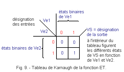
In all other cases, the output VS takes the state 0. One can establish a table, which you already know and which summarizes the different states of VS according to the inputs Ve and that is called : the table of Karnaugh.
Figure 9 shows the table of the AND logic function.
In this figure are represented, at the top, the binary states of Ve1, on the left, the binary values of Ve2.
Inside the boxes, the different binary states of VS.
The truth table is another way of representing the behavior of a circuit. It is illustrated in Figure 10 and constitutes the identity card of the circuit.
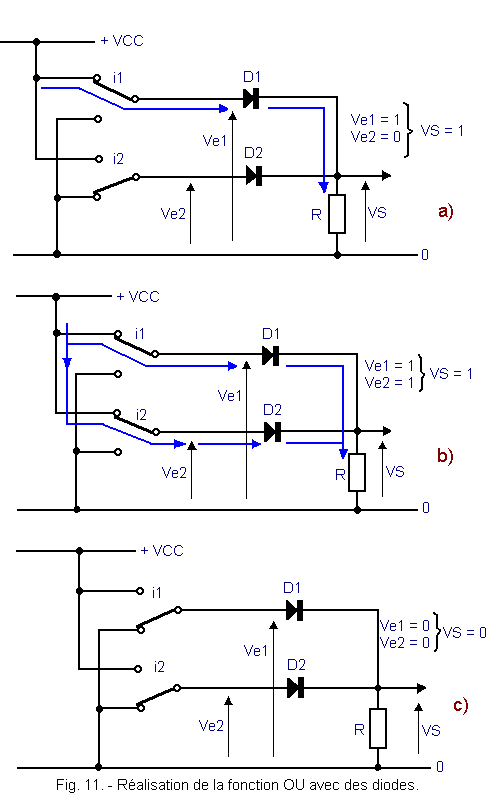
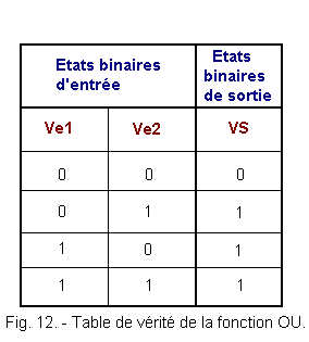
The diagram of this circuit is shown in Figure 11.
The VS output is at state 1 when Ve1 or Ve2, or both are in state 1.
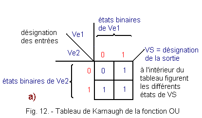
The tables of Figure 12 represent, in different forms, the output states as a function of the input states for the inclusive OR (because it includes the case where Ve1 and Ve2 are in the 1 state).
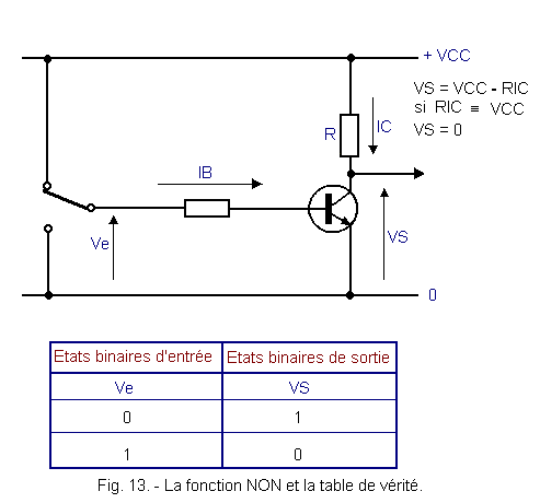
To form a complete logical system, these two previous operators are missing a third, which is the function NO (or function inverter or logical complement).
We have seen that the transistor, mounted as a common emitter, allows this inversion (presence of voltage VBE at the input - absence of voltage VCE at the output).
It is therefore with the assembly of Figure 13 that the function NO is materialized. You will also find his truth table.
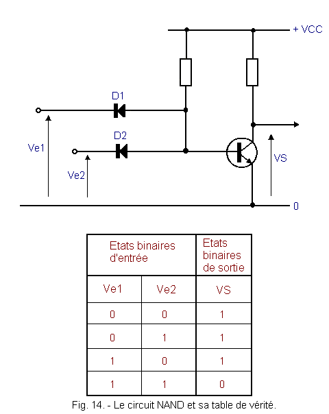
In the case where the NAND (NON-ET) function, for example, has to be performed, the diode AND circuit must be connected, followed by the transistor NO circuit.
The next step is traced, just integrate the diodes and the transistor in the same housing.
This is called D.T.L. (Transistor Logic Diode : logique à diode et transistor).
3. - LOGICAL FUNCTIONS WITH "DTL" DIODES AND TRANSISTORS
3. 1. - THE FUNCTION "NAND"
Figure 14 shows its material realization and its truth table. As you can see, this is the association of the AND circuit previously described (Figure 8), followed by an inverter.
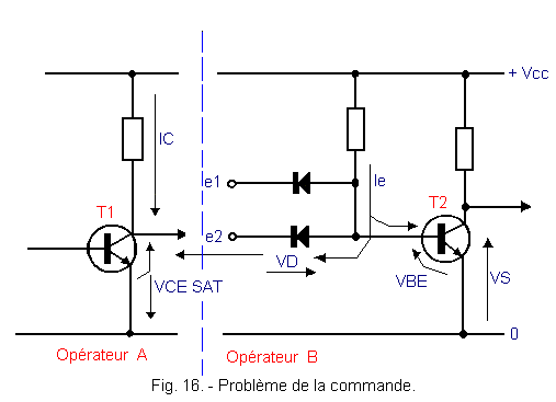
Figure 16 shows the association of an operator A with an operator B.
When the output of the operator A must be in state 0, in fact, it is not quite because the voltage T1 is not a perfect switch and the output is at the voltage VCE SAT (about 0.2 V). To this is added the direct voltage of the diode : VD (about 0.6 V).
The voltage VBE instead of being 0 is at the potential :
VBE
= VD + VCE
SAT = 0,6 + 0,2 = 0,8 V.
This voltage is clearly enough for T2 to drive, whereas it should be blocked.
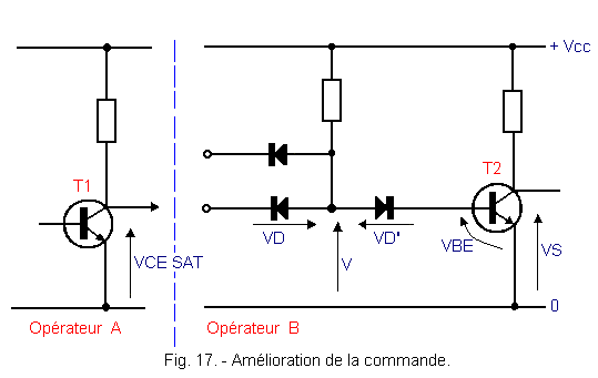
Refer to Figure 17. On the base current path of T2, place a diode. The voltage at its terminals VD', the voltage V is equal to :
V = VD'
+ VBE
When the two operators are together and the output of A is zero, we get :
V = VD'
+ VBE = VD
+ VCE SAT
We can draw :
VBE
= VD + VCE
SAT - VD'
replacing by voltage values :
VBE
= 0,6 V + 0,2 V - 0,6 V = 0,2 V
his voltage is no longer sufficient for T2 to drive and it is blocked.
From now on, we will adopt this change for all DTL operators.
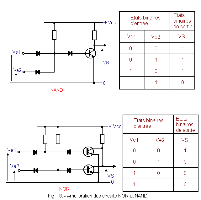
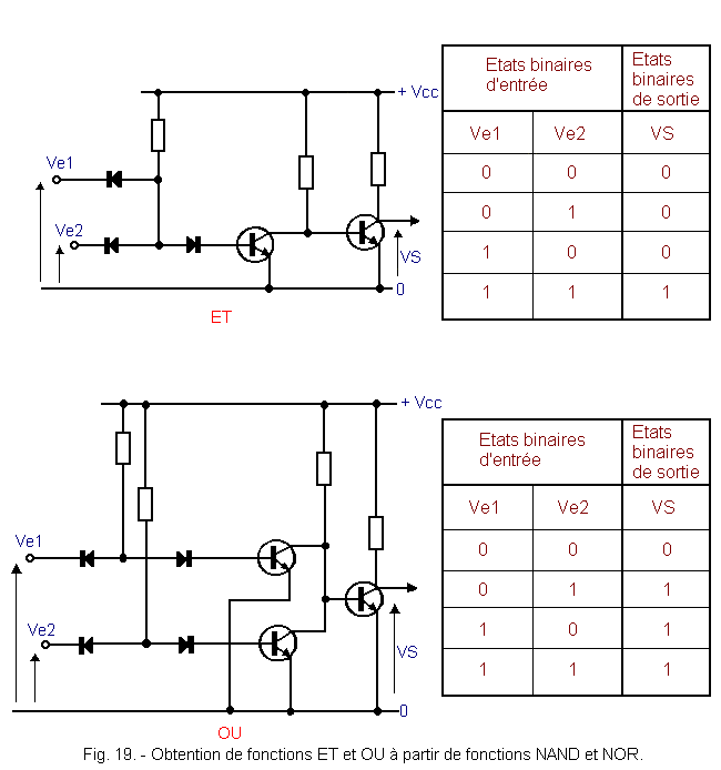
Figure 18 shows the previous circuits by making these modifications.
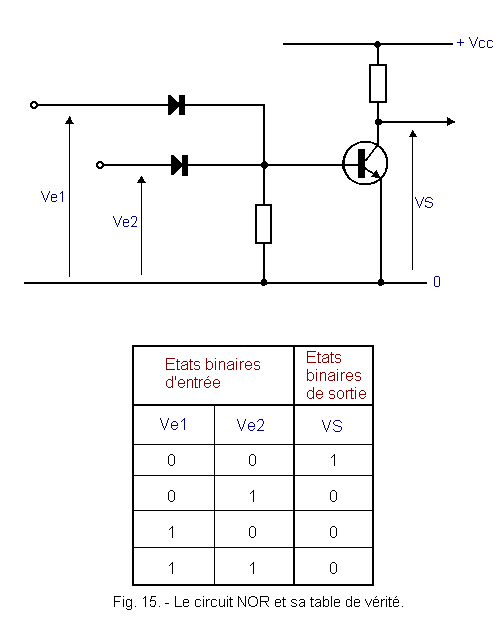
In this figure, the NAND and NOR circuits, followed by an inverter, or NO circuit, make it possible to obtain the AND and OR functions that are shown in Figure 19 as well as their truth tables.
Some manufacturers are still realizing this technology. It is, despite everything, less and less used.


 The OR Function at Diodes
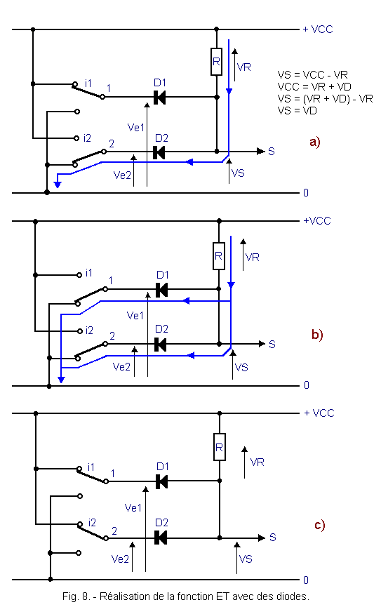
.gif)
 Click here for the next lesson or in the summary provided for this purpose.
 Top of page
 Next Page