Intrinsic and Extrinsic Conduct - The N.P. Junction :
MATERIALIZATION OF LOGICAL FUNCTIONS
INTRODUCTION :
So far, we mainly materialized the binary states using a switch, the latter being open or closed.
The combination of several of these switches makes it possible to perform the logic functions.
This switch consists of an input system and an output system.
Depending on the presence or absence of an action on the input, the output can take two well-differentiated states.
Each of these states being inseparable from one of the input states.
On the other hand, the technology of this switch, or basic element, concerns its realization, its physical materialization. From this materialization flows the origin of the energy that must be applied to the input system to modify the state of the output. It also tells us about the type of usable energy output.
In the case of the switch, the energy used at the input is of mechanical origin, that used at the output is electrical.
This origin may be different, depending on the technology used (pneumatic, hydraulic, electromechanical or electrical).
Depending on the purpose, one technology is used rather than another, for its better qualities.
It is important not to establish a prestigious hierarchy in this choice; it is first question of technical criteria and also of cost price when it is necessary to realize several copies.
These two parameters suffice to understand that there is no definitive choice, but that it can represent an interesting compromise for a given epoch, which is moreover valid in other domains
The realization of logical functions with contacts is still used today in certain sectors such as telephony or some automatisms (elevator control) but it is mainly safe equipment, which always fulfill their function, because the recent achievements are now electronic, services rendered being, moreover, identical.
This contact technology is not suitable for certain uses where the speed of calculation is paramount and where the large number of functions would lead to systems of gigantic size.
Electronics provides a solution to the problem of speed, but the fixtures were very bulky and consumed a lot of energy.
It was not until the advent of semiconductors that digital electronics took off.
We first realized the diodes whose applications were oriented towards logic, then came the transistors for which the applications in this field are numerous.
It only remained to integrate a growing number of transistors on a few square millimeters to lead to the microprocessor, in association with a greater and greater control of logical algebra by a greater number of technicians.
It seems to us essential to detail these steps a little, in order to better dominate the problem. We propose you the following progression :
The semiconductors
The diode and derivatives
The transistor effect
The bipolar transistor
The field effect transistor
The logical functions with diodes
Logic functions with diodes and bipolar transistors
Logic functions with bipolar transistors
Logic functions with field effect transistors
The other logical families
Integrated circuits and their evolution
Circuits used in industry
Lexicon of terms used in builders catalogs
The different kinds of cases.
These different themes are covered in the four technology lessons.
In general, any device using the flow of an electron flow takes the qualifier of electronics.
In these devices, a number of physical principles are implemented to promote the birth of the electron flow. This is then controlled using a signal of the same nature.
Among the different existing bodies, regarding electricity, we can classify them in two categories :
insulating materials, non-conducting electricity
conductive materials, which allow the passage of current.
Between these two limits, semiconductor materials such as germanium or silicon are intercalated.
The first semiconductor devices were made from germanium. Then, silicon was used.
Germanium is derived from the blends from which zinc is also extracted. There are few and it is difficult to produce.
Silicon exists in large quantities since it is derived from quartz and silica. Which explains, in part, the generalization of this material.
1. 1. - REMINDER ON THE CONSTITUTION OF MATTER
The smallest part of a body still retaining the same properties as this one is called the molecule.
The molecule consists of atoms, in varying numbers, depending on the type of molecule.
The atom consists of a central nucleus and electrons that revolve around it in orbits, or layers, the number of which varies according to the atom considered as shown in Figure 1 for germanium and silicon.
The nucleus consists of protons and neutrons. The electric charge of the neutrons is zero while that of the protons is positive.
The electrons have a charge of the same value as that of the protons but of opposite sign, that is to say negative.
The charges of the protons and those of the electrons are balanced, so that the atom is electrically neutral.
The electrons revolve around the nucleus, like our solar system and the planets that compose it.
The successive layers on which these electrons circulate constitute energy levels.
This means that the closer the layer is to the nucleus, the more energy it takes to snatch an electron from it.
It is the last layer, or so-called outer layer of valence, which interests us because it is this which allows the bonds with the neighboring atoms thus allowing the constitution of the molecule. On the other hand, it is on this layer that we can cheat by adding or subtracting an electron.
The electric charge of an atom is neutral. This equilibrium can be broken by subtracting an electron from its peripheral layer. The remaining charge becomes positive. It is said that the atom is ionized positively and it takes the name of cation.
In the opposite case, if an electron is added to the valence layer, the atom is negatively ionized. It takes the name of anion.
The silicon atom has on its peripheral layer, or valence layer, 4 electrons. These allow the connection with 4 neighboring atoms.
At the absolute zero temperature, all these bonds are stable and the material can be considered as insulating.
To tear an electron from its orbit, it must be subjected to a greater force than that which binds it to its nucleus.
This force may be the result of an electric field created by a voltage, or a rise in temperature whose effects are manifested by molecular vibrations. These vibrations result in the application of a system of forces on the electrons whose resultant may be sufficient to tear them from their orbit.
At a temperature of 20° C, the crystal lattice of silicon is the seat of a major thermal agitation.
Electrons are then torn out of their orbits and, in their pathways, they recombine with positively ionized atoms (that is, cations or atoms that have previously lost an electron).
The quantity of free electrons is always equal to the quantity of "holes" ready to accept an electron, because the formation of a hole is the consequence of the departure of an electron.
An increase in temperature results in the formation of an even larger amount of "electron / hole" pairs.
The mobility of these conditions the density of the current flowing in the material (the electric current is a displacement of electrons).
It can be seen, for semiconductors, that when the temperature increases, conductivity does the same.
In germanium, this increase is greater, because the force required to pull an electron from its orbit is lower than for silicon.
1. 3. - EXTRINSIC CONDUCTION
If, in the crystal lattice of silicon, we introduce, in an amount small enough not to modify it, a body whose atoms have 5 electrons on their peripheral layer, these impurity atoms enter the lattice of the crystal lattice, by embedding 4 electrons of their valence layer with 4 adjacent silicon atoms. In this organization, the fifth electron is in "excess". At a temperature of 20° C, the thermal agitation pulls this electron out of its orbit. Thus, the impurity atom becomes positively ionized (cation), since it loses a negative charge, the electron.
However, since these opposite charges are contained in the same volume, the resulting charge is zero.
The thermal agitation acts on the silicon atoms, the intrinsic conduction still exists, but the presence of excess electrons (due to impurities) will tend to recombine the number of silicon atoms that have lost an electron so much faster, in order to reconstruct the mesh.
Finally, there will be only a few missing links in the network. These gaps are outnumbered by free electrons. They carry a positive charge. To restore their balance, they must accept an electron.
In this type of material, they are the minority carriers or acceptors (these are the holes).
In contrast, the impurity atoms that have released an electron are called donors. These electrons, in greater numbers than the holes, are said to be in the majority and since they carry an electric charge (negative), they will be called : the majority carriers.
This operation, which consists of injecting impurities into the silicon (or into the germanium), takes the name of : doping.
The result of the doping that we have just described is called :
N-type conductivity, in which the majority carriers are electrons, minority carriers, holes.
Parallel reasoning can be held by injecting trivalent impurity atoms (3 electrons on the valence peripheral layer) into the crystal lattice of silicon. In this case, each impurity atom associates with 4 adjacent silicon atoms, but an electron in this mesh is missing. This is a place, or hole, likely to receive an electron.
The thermal agitation, leading to the intrinsic conduction, provides the electron to this vacant place, in order to reconstitute the mesh, thus creating a negatively ionized atom (anion).
It follows that the free electrons, in this case, are outnumbered by the holes, they will take the name of minority carriers. The atoms that released them are the donors (which after this operation become positively ionized, they are cations).
The holes, with this type of doping being the majority, take the name of majority carriers, and the atoms to which they belong are the acceptors.
The injected impurity atoms are electrically neutral. When they capture an extra electron, they charge negatively, but this charge is compensated by the creation of another, opposite sign, due to the departure of this electron from a neighboring atom.
The whole remains electrically neutral. This doping makes it possible to obtain :
Conductivity type P, in which the majority carriers are the holes, the minority carriers, the electrons.
In summary, the N or P conductivity materials are electrically neutral N
In the material P, everything happens as if we had injected holes or majority carriers. Some free electrons remain, due to the thermal agitation, they are the minority carriers.
In the material P, everything happens as if we had injected holes or majority carriers. Some free electrons remain, due to the thermal agitation, they are the minority carriers.
It should be emphasized, for what follows, that the holes do not move in the crystal lattice. Only the electrons, which are material elements, move.
The consequence of the departure of an electron is a gap or hole at the location it previously occupied. There is thus an electron flow in one direction and the appearance of a displacement of holes in the opposite direction.
In the descriptions we made, we talked about bonds between atoms. There are many ways for atoms to bond with each other. In the present case, these are covalent bonds (or valence bonds).
If one associates, side by side, a material of type N with a material of type P, we make a junction.
This designates the thin zone in which the conductivity goes from type N to type P (or vice versa).
Let's take a look at what happens at this junction in the following cases :
- without polarization
- with reverse polarization
- with direct polarization
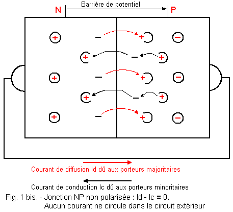
1. 4. 1. - NON-POLARIZED JUNCTION (Figure 1 bis)
In Figure 1 bis as well as in Figures 2 and 3 which follow, a number of signs have been used and that we will detail now :
Material N
- Pentavalent atom of impurity, injected into the silicon. With the agitation, this one becomes :
- a free electron.
- a cation entering the mesh. In the drawings, for clarity, only free electrons and cations will be shown.
Material P
- trivalent atom of impurity, injected into silicon. With thermal agitation, it captures the missing electron to enter the mesh and becomes :
- anion entering the mesh
In both materials, we also find :
- silicon atom of the mesh having lost an electron by thermal agitation
- free electron escaped from the silicon atom.
a) - The diffusion current
The majority carrier electrons of the N zone diffuse into the zone P where they recombine with the majority carriers of this zone, taking place in the holes.
There is an imbalance of the electric charges, indeed, in the zone N, the electrons having disappeared, the charge of the donors or positive ions (cations) is not counterbalanced anymore and this zone becomes positive.
The contribution of electrons in the vacancies of the zone P modifies the electrical equilibrium of this zone with appearance of negative ions (anions).
The displacement of electrons from the zone N towards the zone P is called : diffusion current.
It is accompanied by a positive space charge on the material side N and an equal load but of opposite sign on the material side P. These create an electric field
b) - Conduction current
The effect of this electric field e
will force the minority carrier electrons of the zone P to flow towards the gaps or minority carriers of the zone N, tending to counterbalance the lost charges by diffusion current.
A current of electrons is established from the zone P to the zone N. This is due, in this case, to the minority carriers of these zones.
The junction is the seat of two equal but opposite currents. There is no current flowing in the external circuit.
The zone in which the electric field e
born is called :
c) - Potential barrier
In this zone, the concentration in carriers becomes identical to that of the intrinsic conduction (at equal temperature)
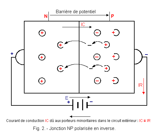
1. 4. 2. - POLARIZED JUNCTION IN THE REVERSE DIRECTION (Figure 2)
Now apply the negative pole of a battery on the electrode of the material P and the positive pole on the material N.
The electric field created by the application of the voltage of this battery is in the same sense as the electric field e of the potential barrier.
These two fields add up and promote the circulation of electrons or minority carriers of the conduction current. In addition, the free electrons of the zone N and the majority carriers of the zone P (the holes) under the effect of this field, will deviate from the junction.
It follows that the cation concentration of the zone N and anions of the zone P will increase near the junction.
The potential barrier is widened and the circulation of electrons, majority carriers, is deficit compared to that of the minority carriers, especially as the e field increases. A limitation of this current is established because the departure of the electrons of the zone P and their arrival in the zone N, create a load of space which limits this current by countering the increase of e.
It circulates therefore a weak current in the external circuit. At constant temperature, for an increase in the voltage of the battery so an increase in E, the current remains virtually constant because it is due to minority carriers from thermal agitation.
Beyond a certain threshold, it is found that the current increases abruptly.
The increase of the field E confers on the electrons of the conduction current a speed such that their kinetic energy reaches a value sufficient so that, in case of shock, with an atom encountered on their trajectory, it tears an electron from it creating thus an increase of free electrons. These electrons are added to the first and the effect becomes cumulative.
This phenomenon takes the name of avalanche effect. It is used for some devices like zener diodes.
In a junction that is not made for this purpose, it causes the irreparable destruction of the junction by breakdown.
The voltage that creates the electric field E for which the phenomenon occurs takes the name of :
- reverse breakdown voltage or avalanche voltage.
Below this voltage, if the temperature is increased, at constant voltage, the thermal agitation increases and the current of the minority carriers does the same. So the reverse current increases. This is an important fact to remember. We will talk about this later in the diode and transistor sections.
The breakdown voltage is called : VRM
(R = reverse = inverse, M = maximum)
- The conduction current due to the minority carriers, the junction being reverse biased, is called IR (R = reverse = inverse).
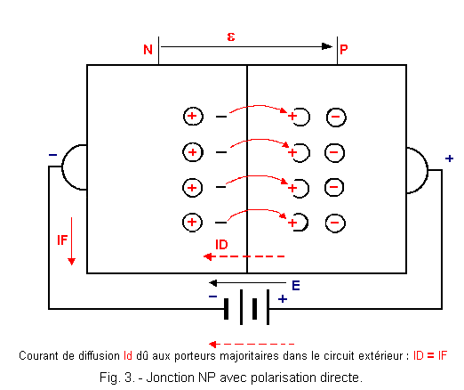
1. 4. 3. - POLARIZED JUNCTION DIRECTLY (Figure 3)
At a low value of the voltage corresponds a weak electric field E, directed in the opposite direction of the field e.
These two fields are opposed and the result is a decrease of
une diminution de e.
Since this is the source of the conduction current (minority carriers in the P zone), we observe a proportional decrease in this current. Consequently, the diffusion current (majority carriers of the zone N) will become predominant and a weak current will circulate in the external circuit.
The departure of electrons from the zone N tends to create a charge imbalance in this material immediately restored by the battery, which injects an equal amount.
In the same way, the arrival of these electrons in the zone P tends to create an imbalance in this material (of sign opposite to the preceding one), but the positive polarity of the pile applied on this side, sucks the negative charges in excess, restoring the balanced.
The gradual increase of the voltage does not lead to a significant increase of the current in the external circuit. However, when we reach a certain threshold, whose value remains low despite everything, we see a sharp increase in the current.
The resulting electric field, gives the majority carrier electrons of the N zone (diffusion current), sufficient energy for them to pass through in large numbers, the potential barrier, whose width is now very reduced.
The cell compensates the departure of the electrons from the zone N and favors the arrival of these in the zone P.
Current flow is well established and for a small increase in voltage, there is a large increase in current.
At this value of electric field E, which conditions the sharp increase of current, corresponds a tension which one names :
VD
or VF- (F = forward = direct).
The current flowing in the external circuit and corresponding to the polarization in the direct direction (or passing) is called :
ID or IF
- (direct current)
The temperature has little influence on this current ; only the threshold voltage is affected, we will see how by observing the characteristics of the diode.
Now that you are familiar with the notion of junction, you have to give an order of magnitude to the physical values that were discussed. In addition, the principles described, concerning the various conductions, are schematized in order to allow a sufficient approach for our use.
Silicon was the main topic, since it is now the most widely used semiconductor material (the principle remains the same with germanium).
It should be known that the germanium atom has a core consisting of 32 protons, electric charge + e and neutron (41) of neutral electric charge.
The atom, in general, being electrically neutral, that of germanium possesses 32 protons and also has 32 electrons of electric charge - e.
These gravitate on 4 layers, or orbits, around the nucleus.
If we assign to these layers a number, the nearest of the nucleus being the first, the maximum number of electrons that can gravitate on these layers is given by the formula :
N = 2 n2
With N =
number of electrons on layer n.
n =
number of the considered layer.
Thus, germanium has : 2 electrons on the first layer, 8 on the second, 18 on the third and only 4 on the fourth (which could accept 32).
The silicon atom consists, for its part, of :
protons of electric charge + e
14 neutrons.
Around this core, 14 electrons charge - e. The first two layers are complete, the third one contains 4 (whereas it could accept 18).
See Figure 1.
These two atoms have the same number of electrons on the peripheral layer, but the silicon has one less layer.
It should be noted that the more an electron is on a layer away from the nucleus, the lower the force required to pull it out (at equal temperature) ; which results in a force measured in electron-volt (eV) of the order of 36% lower for germanium than for silicon at a temperature of 27° C.
In the inverse polarized junction, the IR current (due to the minority carriers of the thermal agitation) will be greater in the case of germanium and, any increase in the temperature, will tend to increase this current in greater proportions than for the silicon.
This is an additional reason for the choice of this material, because in the case of the diode (which we will discuss later), this current is somehow a defect.
There has also been talk of doping, or injection of "impurity" atoms.
In P-type conduction, these atoms are trivalent, that is, they have 3 electrons on their peripheral layer. These atoms are : boron (B), gallium (Ga), aluminum (Al) or indium (In).
In N-type conduction, they are pentavalent atoms (5 electrons on the peripheral layer) which are : phosphorus (P), arsenic (As) or antimony (Sb).
The proportion remains very low and of the order of a few atoms of these bodies for millions of silicon atoms. This proportion may be variable as we will see later in order to favor certain phenomena.
On the other hand, we have considered this material (silicon) as pure, which in reality is not the case. In the manufacture of semiconductors, we will endeavor to refine the material at best, so that it contains, as impurities, only those injected.
We talked about the width of the potential barrier, it should be known that it is about 1
micrometer more commonly called micron (1
micron = 1 µm = 10-6 meter), which is already much at the atomic scale. The distance between two silicon atoms is of the order of 10-10
meters (see 1
Å
= 1 angstrom).
It should also be said that if the thermal agitation favors the departure of the electrons from their orbits, these do not remain indefinitely free. During their journey, they meet a place left free, by the departure of a precedent, therefore undergo an attraction because the electric charge of this atom is broken (it is a cation thus positively charged) and there is capture.
This is called the lifetime of the free electron before its recombination within another atom (or rather cation).
It is good to specify that a pentavalent impurity atom, injected into the silicon and entering the mesh, will tend to lose more easily its fifth electron, by thermal agitation, because it does not enter the mesh.
On the other hand, a silicon atom (positively ionized by thermal agitation) or a trivalent impurity atom forming part of the mesh will attract more sensitively its missing electron.
There is much to be said about all these phenomena, but these are the subject of very advanced studies by specialists and go well beyond the scope of this first lesson.
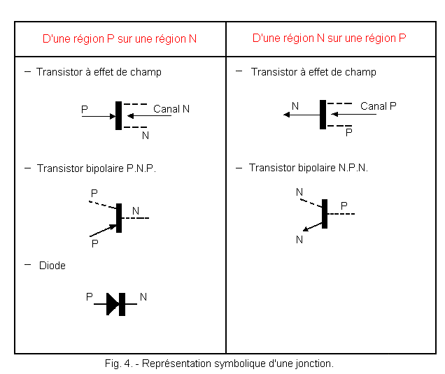
Figure 4 shows the symbols of the different junctions that can be encountered in semiconductor devices.


 Theory of semiconductors
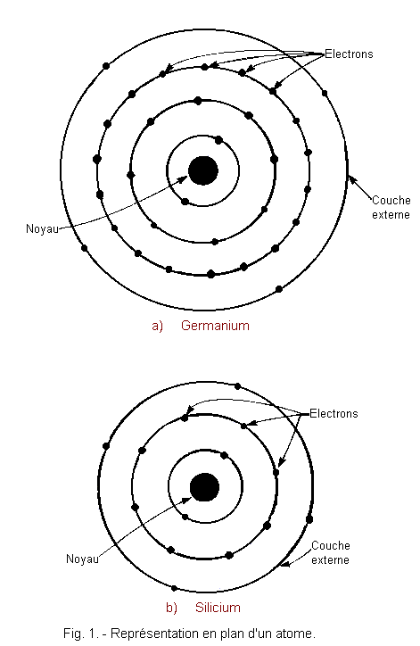
 Click here for the next lesson or in the summary provided for this purpose.
 Top of page
 Next Page