Review of a Reset Toggle - Set (R-S) Made with 2 NAND :
In this 4th practice, you will continue the editing of the digital desk by increasing its possibilities of use thanks to two push buttons. these will generate voltage pulses needed for new experiments. You will also wire a circuit for detecting the rising edges of a signal, see the passage of a voltage from level L to level H.
You will also learn how the scales work. Previously seen circuits (AND, OR, NAND, NOR, EX-OR) are used in the COMBINATION logic.
This term means that the logic level present at the output of the circuit in question is solely a function of the logic levels present at the input at the instant considered. In other words, the logical level of the output does not depend on the previous states of the inputs.
Flip-flops are part of the SEQUENTIAL systems ; the latter make it possible to obtain at the output a logic level which depends on the level of the inputs at the moment considered, but which also takes into account their previous state.
Sequential circuits can be very complex.
The scales are the simplest of them.
We will examine some types of scales made first with NAND circuits and later with unique specialized integrated circuits.
1.
- PREPARATION OF HARDWARE
In order to carry out the exercises proposed, please use the following components (which you will take from the material in your possession) :
2. -
FIRST EXPERIENCE : EXAMINATION OF A RESET - SET (R-S) TOGGLE WITH 2 NAND
Examination of a reset - Set (R - S) rocker realized with 2 NAND.
A flip-flop is a bistable circuit, that is to say characterized by an output that can take two logical states stable in time (L or H) ; the swinging output as soon as one acts on an appropriate input. A flip-flop usually has two outputs Q and .
The two outputs are always at complementary levels : when Q is at level H,
is at level L and vice versa.
Generally, we use the Q output to define the state of the flip-flop. It is said that the flip-flop is in logic state 1 if the output Q is in the logic high state and the flip-flop is in the logic 0 state if the output Q is in the low state.
In this exercise, you will study the simplest rocker : the RESET - SET rocker made with two NAND circuits.
We call SET, the state 1 of the flip-flop and RESET the state 0.
Preparation of three-conductor connecting wires :
a) Cut three pieces of insulated rigid wire : one of about 10 cm and the other two of 5 cm. Strip the ends. Connect the three wires together at one end by twisting them and then welding as shown in Figure 1.
b) Proceed as above, prepare two more three-conductor wires. You can now start the exercise.
c) Remove all links related to the last experiment.
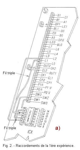
d) Remove from I.C.X. the integrated circuit used previously and replace it by the integrated circuit MM 74C00.
Referring to Figure 2-a, make the following connections :
e) Using two pieces of 5 cm wire, connect pin 1 of the integrated circuit (input of the 1st NAND) to the switch SW0 and pin 5 (input of the 2nd NAND) to the switch SW1.
f) Using the triple wire previously prepared, connect pin 3 (output of 1st NAND) and pin 4 (input of 2nd NAND) to LED L0.
g) With the second triple wire you have prepared, connect pin 2 (input of the 1st NAND) and pin 6 (output of the 2nd NAND) to the LED L1.
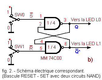
h) Put the two switches SW0 and SW1 on position 1. With the connections made, you realized the circuit illustrated Figure 2-b. As you can see, the circuit has two inputs and two outputs. One entry is designated by the symbol
and the other by the symbol .
The letters S and R are the abbreviations of the terms Set (Write or Reset) and Reset (Clear or Reset).
Both outputs are denoted Q and
because there is a possibility that the two outputs are not complementary. The Q output is the reference output of the circuit.
Now connect the power supply and observe the L0 and L1 LED, one LED will be on and the other off. It is not possible to predict which of the two will light because it depends on the physical characteristics of the two NAND circuits and more precisely their response time. They are never exactly the same.
Since the response time of a logic circuit can vary within a wide range, it is not possible to know which of the two NAND constituting the flip-flop will switch first on power-up.
Set the scale to a specific state at power up, some adjustments are necessary. They will be examined in the following practice.
Check now how the circuit works :
i) Set the SW0 switch to the 0 position. Thus, the
input is at the L level. You can see that the L0 LED connected to the Q output is lit, while the L1 LED is connected to the ,
output is off. This means that the output Q is at a level H and the output
is at a level L.
j) Put SW0 back on position 1, the state of the output is unchanged.
k) Then switch SW1 to position 0. You notice that LED L0 goes out and LED L1 lights up.
l) Put SW1 on position 1. You notice that L0 remains off and L1 on.
With this test, when SW1
()
is set to 0, you see that the output Q (L0) remains unchanged by repositioning SW1 to 1.
m) Perform the same operation with switch SW0 by setting it to position 0. You notice that L0 lights up, while L1 goes out.
n) Put SW0 back in position 1, L0 stays on. When SW0 is set to 0, the L0 LED lights up and stays on when SW0 is repositioned to 1.
When SW1 is set to 0, the L0 LED goes out and remains off when SW1 is set to 1.
Do not position both switches simultaneously at 0.
From previous tests, you can draw the following conclusions :
the two outputs Q and
are always complementary to each other.
whenever the input
is carried, even momentarily at the level L, the output Q is brought to the level H (L0 on) ; a return to level H on
retains the level H in output Q.
We can say that the rocker is "remembered" that the entry
is momentarily passed by the level L.
whenever the input
(SW1) is carried, even momentarily at the level L, the output Q is brought to the level L (L0 off) ; the return of the level H on
has no influence on Q which remains on the level L.
We can say that the rocker is "remembered" that the entry
momentarily went to the level L.
in the end, the rocker "recalls" which of the two inputs was last taken to the level L. It remains in the corresponding state indefinitely until the other input is brought to the level L.
an input is called "active" when it determines a switchover of the state of the two outputs.
the fact that the two inputs are active in the low state is indicated by the bar placed above the "symbols" R and S (
and ).
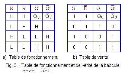
As with all combinational logic circuits, the operation of the flip-flop can be described by the operating table and the truth table.
The operating table can be established on the basis of the tests carried out previously.
When both entries
and are both brought to level H, the rocker does not change state.
The state of the outputs is determined by one of the two inputs previously brought to the level L. This condition is generally represented by "Q0" and "0",
which you find in the first line of the operating table of the Figure 3-a.
In the last line of the table, there is a combination of input levels that has not been tried so far. This is the case where both inputs are at level L.
To see what happens in this case, do the following :
a) Put the two switches SW0 and SW1 on position 0. You notice that L0 and L1 are both lit.
This is contrary to the conventional operation of a rocker that usually sees its outputs take additional levels.
b) By simultaneously positioning the two switches SW0 and SW1 on 1, you will see that one of the two LEDs goes off, depending on which input reaches the first level H.
As a result, the state of the latch is indeterminate when the two inputs positioned at L are brought to a level H (state of rest). This is why this combination (
= 0 and = 0) of the input levels is undesirable.
In Figure 3-b, you are shown the truth table of the RESET - SET flip-flop. You immediately move from the operating table to the truth table by associating the logical digit L with the digit 0, the logical level H with the number 1.
In summary, the RESET-SET flip-flop, often referred to as R-S, is a memory element that has the following characteristics :
the two entries
and
are in the state of rest when they are at level H.
a logic level L applied on
switches the output Q to a level H : this state is also said SET.
a logic level L applied on
switches the output Q to a level L : this state is also said RESET.
a logic level L applied on the two inputs
and
switches the two outputs to a level H. When the two inputs return to the state of rest (H), the rocker goes to an indeterminate state. So the LL input combination is undesirable.
finally, the R-S latch makes it possible to store the passage at the level L of one of the two inputs.
The jobs of this circuit are multiple, as you can realize by continuing the manipulations.


 Examination of a reset-set rocker made with 2 NAND
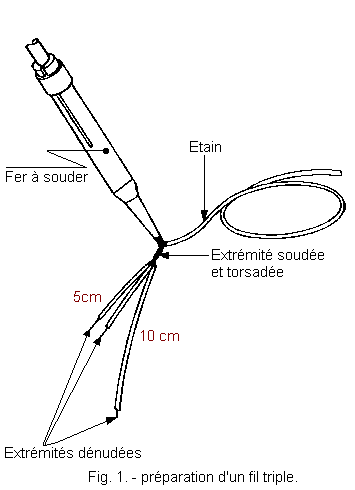
 Click here for the next lesson or in the summary provided for this purpose.
 Top of page
 Next Page