Application of Exclusive OR Circuit and NAND Circuits, NOR ... :
5. - THIRD EXPERIENCE : REVIEW OF A CIRCUIT OR EXCLUSIVE
You will now use the integrated circuit MM 74C86 with 4 Exclusive OR circuits as you can see in the wiring diagram of Figure 12.
Since the two inputs and the output of the first exclusive OR circuit to be tested do not match the NOR circuit terminals discussed above, you must make new connections as follows :
a) Disconnect the power supply and remove the connections related to the previous experiment.
b) Remove the integrated circuit MM 74C02 of the ICX support and insert in it the integrated circuit MM 74C86.
c) Connect the points indicated below :
pin 1 of the integrated circuit MM 74C86 and the contact SW0,
pin 2 of the integrated circuit MM 74C86 and the contact SW1,
pin 3 of the integrated circuit MM 74C86 and the contact L0.
d) Put the two switches SW0 and SW1 in the position corresponding to the symbol 0, so the two inputs of the exclusive OR circuit are both at the level L.
e) Feed the circuit again,
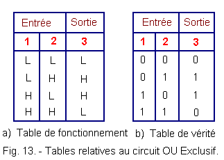
Now you can check the operation of the circuit in question, proceeding as for previous experiments. Check for each of the four possible combinations of the levels of the two inputs, the corresponding output level. Write the operating table and then the truth table in positive logic of the Exclusive OR circuit. Then compare the results obtained with those given in the two tables of Figure 13.
Looking at the operating table in Figure 13-a, you will find that the main feature of the Exclusive OR circuit is to give an output at the H level when the two inputs are at different levels. When the inputs are both at the same level L or level H, the output is at level L.
Because of this operating characteristic, the Exclusive OR circuit is sometimes used as a difference detector.
5. 1. - AN APPLICATION
OF THE CIRCUIT OR EXCLUSIVE
You will now perform an exercise how an Exclusive OR circuit can find applications as a controlled inverter.
In other words, you will check how in practice, by using one of the two inputs as control input, at the output of the Exclusive OR circuit you get the signal present on the other input, inverted or not according to the level that is on the order entry.
Suppose you use the input connected to pin 1 as the command input :
Leave unchanged the connections made during the previous experiment and put the two switches SW0 and SW1 on the position corresponding to the symbol 0 ; thus, entry 1 as well as entry 2 are at level L.
By observing the LED L0, you see that it is off which means that the output of the circuit is at voltage level L.
Now turn input 2 of the circuit to level H by switching SW1 to position 1.
This time you see that the LED L0 lights up, which indicates that the output is at level H. You can thus observe that with the command input at level L, the output is at the same level as input 2.
Then put control input 1 on level H, by switching SW0 to the position indicated by symbol 1.
Set switch SW1 alternately to position 1 and position 0, thus successively applying to input 2 an H level or a L level.
By observing the LED indicator L0, you can see that when input 2 is at level H, the output is at level L and vice versa. The demonstration is thus made that in this condition, that is to say with the control input at the level H, the Exclusive OR circuit outputs an inverted signal with respect to that present at the input 2.
In summary, the Exclusive OR circuit can operate as a controlled inverter by using one of its two inputs as control input. If input 1 is used as the control input, it is at level L, the Exclusive OR circuit does not reverse the signal applied to input 2 ; while with input 1 at level H, the circuit outputs an inverted signal compared to that applied to input 2.
Similar operation is achieved using input 2 as the control input. In this case, if the control input 2 is in the L state, the output is at the same level as that present on the input 1 ; while if the control input 2 is in the H state, the output is always at a level opposite to that of the input 1.
6. - FOURTH EXPERIENCE : USE
OF AN INTEGRATED CIRCUIT NAND
TO REPLACE OTHER TYPES OF CIRCUITS
Often in the same assembly are circuits of different types : OR, NAND, Inverters, etc. ...
In some cases, it would be expensive to use a different integrated circuit for each type of function to perform.
If, for example, an assembly requires the use of a single inverter and a single NAND gate, it would be uneconomical to use a MM 74C04 as inverter and a MM 74C00 for the NAND circuit.
Indeed, one sixth of the integrated circuit MM 74C04 (which contains 6 inverters and a quarter of the integrated circuit MM 74C00 containing 4 NAND) would be used. It is therefore useful to be able to substitute certain circuits by others performing the same function.
The equivalences between the different circuits have already been studied in the Digital Electronics Theory of the 3rd lesson. In the following experiment, you will check how it is possible, in practice to perform some logical functions using NAND type circuits instead of specific integrated circuits.
a) Disconnect the power supply and remove all connections related to the previous experiment.
b) Remove the integrated circuit MM 74C86 from the ICX support and insert in it the integrated circuit MM 74C00.
As you have already learned in the previous practice, the integrated circuit MM 74C00 includes 4 NAND circuits, each of them having two inputs and one output.
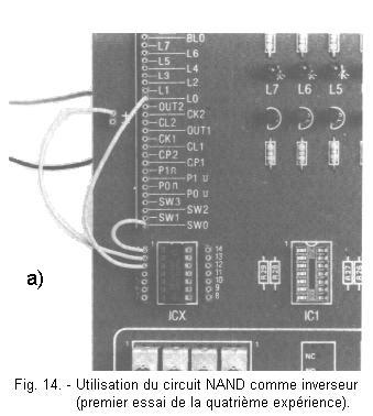
c) Using the pre-prepared pieces of wire you have, make the connections shown in Figure 14-a.
In this way, the input 1 is connected to SW0 while the input 2 is connected to the positive voltage (level H). The output of the NAND circuit is as usual connected to the L0 indicator.
First try
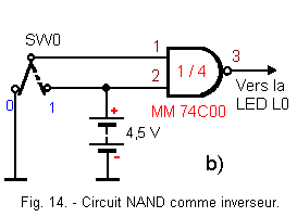
a) Put SW0 on position 0, you realize thus the circuit represented Figure 14-b.
b) Connect the power supply, observe the LED L0 : you notice that it is lit.
c) Then put SW0 in position 1. Note that LED L0 goes out.
You can therefore conclude that : if input 1 is at level L, the output of the NAND circuit is at level H (LED on) whereas if input 1 is at level H, the output is at level L (LED off). The NAND circuit connected as shown in Figure 14-b thus behaves like an inverter.
Since the two inputs of the NAND circuit are interchangeable, the same result is obtained by keeping the input 1 permanently at the level H. In this case, the circuit behaves like an inverter, that is to say that the output is at a level opposite to that applied to input 2.
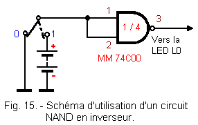
The operation of an inverter NAND circuit can also be obtained by connecting the two inputs as shown in Figure 15.
In practice, this solution has not been adopted solely for convenience of connection, but you can keep it in memory and use it when needed.
Through this test, you will verify that it is possible to perform the OR function using only NAND gates.
a) Disconnect the power supply from the circuit,
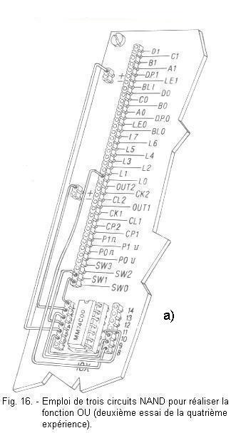
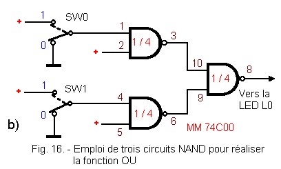
b) Remove the link between pin 3 of the integrated circuit MM 74C00 and contact L0, leave the connections of pins 1 and 2 corresponding to the two inputs of the first NAND circuit.
c) Connect with a piece of wire of about 5 cm, one input of the second NAND circuit (pin 4) to contact SW1 and with a piece of wire of about 15 cm, the other input (pin 5) of the same circuit to the second contact +. Through these links, the first and second NAND circuits provide the function of inverters.
d) Using two pieces of wires of about 5 cm, connect the output of the first NAND circuit (pin 3) to one of the inputs of the third NAND circuit (pin 10) then the output of the second circuit (pin 6) at the other input of the third circuit (pin 9).
e) With a piece of wire of about 10 cm, connect the output of the third circuit (pin 8) to LED L0.
f) Set SW0 and SW1 to the position corresponding to the 0 symbol.
With the connections made, you have just realized the circuit represented Figure 16-b.
Note in this circuit the absence of the symbol of the power stack shown so far in the diagrams. The connection at level H is designated by the sign "+" in order to simplify the drawing. This simplification is commonly practiced for the elaboration of electrical diagrams of logic circuits.
Now you can reconnect the power supply and check yourself the operation of the circuit realized by proceeding exactly as for the previous experiments.
Realize all the possible combinations of the input levels of the circuit by acting on SW0 and SW1 and check for each of them the indication of the state of the output concretized by the LED L0.
You notice that the operation of the circuit corresponds to the tables of Figure 17.
Comparing these two tables with those established in previous experiments on different types of circuits, you notice that they are exactly the same as those of the OR circuit.
Whenever you have to make a circuit that provides the OR function, that is, the logical sum of digital signals, remember the circuit you just experimented with.
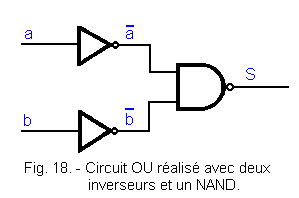
This circuit can be realized with 3 NAND circuits as you have just seen, but it can be done with two real inverters connected to the inputs of a NAND circuit as shown in Figure 18.
By designating the two logical variables applied to the input with the letters a and b, and by S the output variable, the logical function performed by the circuit can be written in the form :
S = a + b
7. - FIFTH EXPERIENCE : USE OF THREE NOR
CIRCUITS TO REPLACE A CIRCUIT AND
In the previous experiment, you have seen how an OR circuit can be realized with three NAND circuits or with two inverters and a NAND circuit. You will now experimentally verify how an AND circuit can be replaced by three NOR circuits or two inverters followed by a NOR circuit.
a) Disconnect the power supply, remove the integrated circuit MM 74C00 ICX support and remove the connections related to the previous experience.
b) Take the integrated circuit MM 74C02 and insert it into the ICX holder. As you have seen previously, this integrated circuit internally contains 4 NOR circuits.
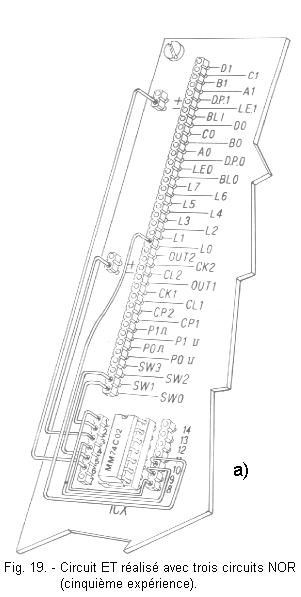
c) Make the new connections shown in Figure 19-a.
d) Place SW0 and SW1 on position 0. You have just completed the circuit shown in Figure 19-b.
e) Power the circuit and observe the LED L0.
Given that the L0 LED off indicates a low level (L) at the output of the circuit and the high level LED (H) illuminated, you yourself constitute the operating table of the circuit in question by realizing by means of SW0 and SW1 the four possible combinations of voltage levels H and L applied to the inputs.
From the operating table, then determine the truth table in positive logic (remember that level H is associated with logic level 1 and level L with logic level 0).
The possibility of making an AND circuit using three NOR circuits may be useful in the case where NOR circuits are available, you would not intend to specifically add an integrated circuit to realize a single AND circuit.
With the aid of three NOR circuits, it is therefore possible to make an AND circuit to replace an integrated circuit MM 74C08.
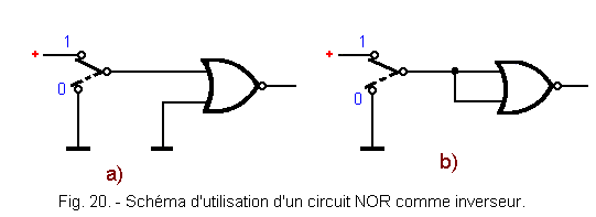
Note that in the realized circuit (Figure 19-b), the two NOR circuits having one of their two inputs permanently connected to ground (L level) perform the function of inverter.
Finally, since
an AND circuit can fulfill the function of inverter when one of the two inputs is permanently at the level H (first test of the fourth experiment) in the same way a NOR circuit can fulfill the function of inverter in the case where one of its inputs is permanently at the level L as indicated figure 20-a. The same result is obtained by connecting the two inputs to each other as you can see in Figure 20-b.
Taking into
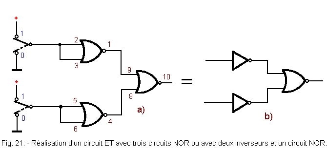
account the above, the result of the fifth experiment can be obtained not only with the circuit shown in Figure 19-b,
but also with the circuit of Figure 21-a or by replacing the first two NOR circuits operating in inverters by two true inverters as shown in Figure 21-b.
With this practice, we have completed the review of fundamental logical integrated circuits.
You have been able to identify their characteristics in practice and to make interesting experiments demonstrating how it is possible to obtain equivalent logical functions by using integrated circuits of different types.
In the next practice, you will expand your knowledge on these circuits as well as the R.S. flip-flops for example and many others.


 An Exclusive OR Circuit Application
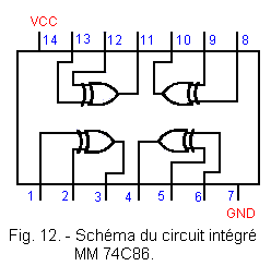
.gif)
.gif)
 Click here for the next lesson or in the summary provided for this purpose.
 Top of page
 Next Page