The Logic Simulator, How to make a good cabling ? :
NOTE :
From the largest computer to the smallest pocket calculator, digital technology is there. It develops every day more and intervenes in every area of your modern life in which electronics is present.
The purpose of the practical experiments of digital technique and to allow you, by means of manipulations, to study the fundamental principles of this technique.
Through a series of practical exercises programmed in a progressive way, you will be able to assimilate easily the notions exposed in the theory; you will learn at the same time the function and use of the various electronic components commonly used in the industry, by performing experimental setups.
The knowledge you will have acquired basic circuits, can be expanded later, offering you the opportunity to specialize in this technique ; for the purpose of constructing, repairing and controlling any apparatus using digital technology.
You will find all electronic components, resistors, capacitors, integrated circuits, transistors, etc ... in any e-commerce. It will be enough to choose the correct components but we will give you all the characteristics of each practice, that is to say the values of resistors with marking and capacitors and many more in order to facilitate your practical work.
Only part of the material of this first practice will be used immediately for exercises ; the remainder will be used later, with the complementary material of the next series ie the 2nd practice, the 3rd, etc. ...
It is therefore advisable to separate the components whose use is not immediate and place them in a safe place.
For the execution of montages, follow scrupulously as and when the indications provided, even if sometimes some may seem superfluous ; in this area, controls are never too numerous and even less useless.
IMPORTANT NOTE :
Do not remove the integrated circuits from the antistatic foam (or antistatic holster) before using them immediately as they may be damaged irretrievably.
For convenience, we will trace the electronic diagrams partially to each practice to better understand and we will explain their various operation and finally to simplify your work as well as experimental setups.
Any similarity to our project, we would be irresponsible. However, the logic simulator should not be marketed without our agreement under pain of sanction because this site is completely free.
For those or those you have the attention to make the circuit boards of the Digilab, you can ask them at this address, by asking for a quote : Quotation request
In this practice, you will begin the assembly of the simulator console illustrated in Figure 1 entitled "DIGILAB" which will allow the development of the program of practical experiences planned in our project.
You will have the opportunity to appreciate at the end of editing the usefulness and convenience of use of "Digilab" in the verification of the operation of different types of integrated circuits or in the experimentation of an electronic circuit. Indeed, for a didactic purpose or simply for fun, it allows to perform quickly relatively complicated experimental setups, without requiring the use of soldering iron and avoiding the difficulties usually encountered when one does not have a suitable support for the circuit that is desired to achieve.
Finally, making possible the realization of test circuits of all kinds, the logic simulator can be transformed into a control device and test, useful for the individual verification of the integrated circuits which are constituted devices based on the digital technique.
1. 1. - GENERAL CHARACTERISTICS OF THE SIMULATOR
It is in the form of a box whose upper face comprises 2 areas (Figure 1).
On the right zone are the following elements :
Hexadecimal display set
It is formed by two hexadecimal displays with 4 x 7 points matrix with decoder circuit and built-in memory allowing the visualization of hexadecimal coded digital signals which we will discuss later.
LED indicator set
Formed by 8 LEDs and their control circuit, this set provides a visual indication of the logic levels present at different points of the circuits studied.
Connector group
This set of connectors consists of 42 contacts allowing access to all functions of the simulator by simply inserting (without welding) the rigid son constituting the links.
Double clock oscillator
It consists of two oscillator circuits with resistance and capacitance (RC), independent of each other, able to provide rectangular signals having the following frequencies :
first oscillator : 1
Hz, 10 Hz, 100 Hz
second oscillator : 1
kHz, 10 kHz, 100 kHz.
As the two oscillators are independent, two signals of different frequencies : one provided by the first oscillator and the other by the second will be simultaneously available on the group of connectors.
The switching of the frequencies of each oscillator is done by the selection of resistors of appropriate values.
State change detector
This circuit makes it possible to carry out checks on the digital signals, it allows, more precisely, to check the moment when a signal passes from one state to another.
Set of mechanical inverters
The set of inverters consists of four switches with 2 positions to have as many logic control variables ; by actuating them, it is indeed possible to change the logical state of each variable by switching a high state (1) or a low state (0).
Set of push buttons
This set is equipped with an anti-rebound system, allowing to have on the group of connectors, rising edges or descent free of the phenomenon of rebound due to the mechanical elasticity of the contacts which we will discuss later.
Support for integrated circuits
This support, with 14 pins for integrated circuit, connected to the connectors, will allow to realize the first experiments on logical circuits by which you will be able to concretize the theoretical explanations.
In the left area are the controls for the power supply circuit that the simulator is equipped with, as well as the contact matrix for experimental setups.
Matrix with contacts
On this plate, one can carry out the assembly and the tests of electronic circuits without having to perform welding. It is thus possible to modify the circuit or to recover the components after the experiment. If a soldering iron had been used, the reliability of the components could have been compromised.
Speaker socket
This jack gives access to a loudspeaker placed inside the cabinet.
On / off switch
This switch is used to apply the mains voltage to the power supply circuit of the simulator placed inside the cabinet.
The electrical characteristics of the power supply are as follows :
Input voltage : 220 V
Output voltage : 5 V
Intensity of the maximum output current : 1,5 A
Protection of the output against short circuits
Internal protection against thermal overload.
Nomenclature for the construction of the logic simulator is as follows :
1 circuit board 17 x 18 cm and adhesive strips of 1.5 mm (approximately)
1 x 4.5 V battery
10 resistors 220 Ω - 1 / 4 W tolerance ± 5% (red - red - brown - gold)
9 resistors 15 kΩ - 1 / 4 W tolerance ± 5% (brown - green - orange - gold)
6 resistors 4.7 kΩ - 1 / 4 W tolerance ± 5% (yellow - purple - red - gold)
1 resistance 12 kΩ - 1 / 4 W tolerance ± 5% (brown - red - orange - gold)
2 resistors 150 kΩ - 1 / 4 W tolerance ± 5% (brown - green - yellow - gold)
2 resistors 1.5 MΩ - 1 / 4 W tolerance ± 5% (brown - green - green - gold)
1 tantalum electrolytic capacitor of 0,33 µF - 10 V
1 ceramic capacitor disc of 330 pF
8 LEDs of 6 mm
10 transistors BC 238B
3 standard type supports for integrated circuits (14 pins)
3 professional type supports for integrated circuits (14 pins) 2 for displays + 1 for ICX
1 integrated circuit MM 74C74
1 integrated circuit MM 74C14
1 integrated circuit MM 74C00
2 hexadecimal displays with 4 x 7 points matrix type TIL 311 or its equivalent
2 connectors with 32 contacts online
2 alligator clips with cap (1 black and 1 red)
1 braid of soft red - black threads (approximately 30 cm each)
8 screws f
3 x 6 mm
4 hexagonal threaded spacers
1 solder roll
4 switches with two positions (inverters)
2 pushbuttons (inverters)
The aforementioned components are reserved solely for the assembly of the Printed Circuit, with regard to power supply, transformer, fuse, regulator, cabinet, etc. ... will be given to you in the following practices including some integrated circuits for the digital experiences.
2. - COMPONENTS USED IN THIS PRACTICE
1 circuit board 17 x 18 cm and adhesive strips 1.5 mm wide (approximate)
1 x 4.5 V battery
8 resistors 220 Ω - 1 / 4 W tolerance ± 5% (red - red - brown - gold)
6 supports for integrated circuits 14 pins (3 standards + 3 of the professional type)
2 connectors with 32 contacts online
2 alligator clips with caps (1 black and 1 red)
8 LEDs (light-emitting diodes)
1 braid of soft red - black (about 30 cm)
4 screws f
3 x 6 mm
4 hexagonal threaded spacers
1 solder roll
You must have a screwdriver, tweezers, cutting pliers, soldering iron and a universal controller.
We measured the pros and cons of designing the logic simulator project on several practices as well as the experimental setups ; because we are aware that some people will not be able to trace tracks with tape on the circuit board or buy virtually all components. But however, we have done everything to facilitate the tasks.
You can also visit the sites that are specialized in the field of manufacturing circuit boards in single or double-sided (tracks with adhesive tapes), by asking them for a quote via the search engines by typing in the "Circuit" area "printed".
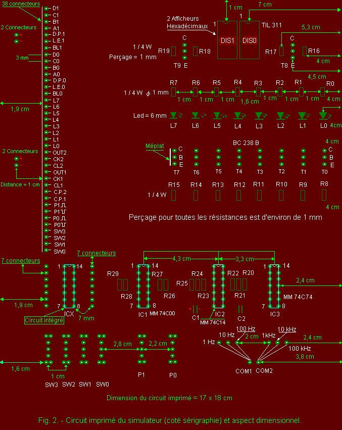
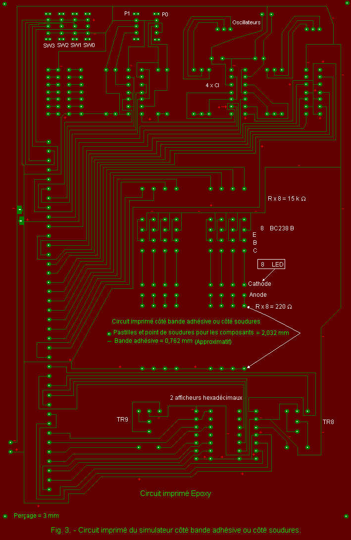
In fact, this circuit board is not very complicated because by looking more closely as you can see in Figures 2 and 3, the same circuit is on the upper face (or screen printing side) indications on the location of components (Figure 2) while Figure 3 shows the stripes of adhesive or copper strips to which we have deliberately spaced the pellets and adhesive strips to better distinguish so as to be able to draw correctly on a printed circuit board size 17 x 18 cm. It is obvious, between two adhesive strips has a separation of 2 to 3 mm and this, to avoid any short circuit.
For those or those you have the attention to make the circuit boards of the Digilab, you can ask them at this address, by asking for a quote : Quotation request
Figure 2 shows the location of the components and the dimensional aspect.
Figure 3, for its part, illustrates the traces of tape or copper on a circuit board, it is sufficient to trace them for personal use.
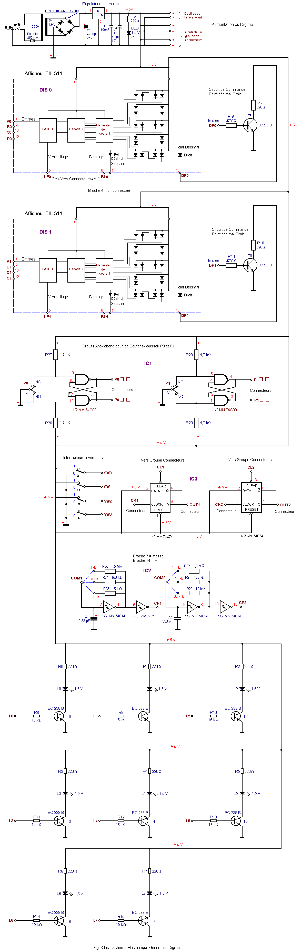
Figure 3-bis, represents the general electronic diagram of the Digilab, so that you can make your artwork that is already drawn, "Figures 2 and 3".
The use of the supports for the integrated circuits offers the advantage of being able to use these without having to solder them, thus, if necessary their replacement will be easy and fast.
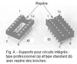
There are two types of media. They differ from each other by the technique of making pins, shown in Figure 4.
Three of the supports that you will use in this practice are professional type (Figure 4-a) with tulip contacts obtained by turning. They are particularly suitable for integrated circuits with fairly thin and fragile pins. This type of contact is able to ensure a better connection from the electrical point of view, even after many insertions of the component.
The other three supports are standard type (Figure 4-b) suitable for everyday use.
For a correct mounting of these supports, carefully read the notes on their orientation, because according to the manufacturers, the reference system of pin 1 differs somewhat (Figure 4).
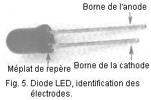
The LEDs are provided with two electrodes (anode and cathode) to be correctly identified at the time of mounting : otherwise, the LEDs may be damaged.
Figure 5 shows you how to distinguish the cathode from the anode of an LED.
Before starting the work of editing, it is good to draw your attention to some remarks that will allow you to make good welds.
As you may have noticed by observing the underside of the circuit board (copper side, Figure 3), the pellets on which you must perform the welds are in most cases very close. It is therefore necessary to use a soldering iron with a very fine tip ; moreover, the power of the soldering iron must be between 15 and 25 Watts so as not to damage the pellets or the components to be welded. The iron will be equipped with an isolation transformer or will be disconnected during soldering.
It is also essential to use good quality tin solder with a diameter of not more than 0.75 mm.
The equipment you have at your disposal or buy recently must meet these requirements perfectly ; under no circumstances should you use solder or a soldering iron that does not meet the requirements listed above.
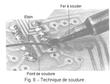
After each soldering point (Figure 6), be sure to clean the tip of the soldering iron tip with a sponge (or cotton cloth) that is kept constantly moist.
To perform a good weld, practice as follows :
press the tip of the soldering iron so that the tip touches the component terminal and the copper solder pad at the same time.
put the end of the tin at the precise point where the solder terminal is in contact with the tip of the tip and hold it in this position until a sufficient amount of tin has melted to form a drop the size of the pellet.
keep the soldering iron in contact with the pad and the terminal the time necessary for the tin to spread well on the pellet and to coat the terminal to be welded ; this time can vary from 3 to 5 seconds.
Avoid keeping the soldering iron too long in contact with the soldering point as otherwise you risk damaging the copper track or component.
During these operations, it is good to slightly move the tip around the point to be welded to promote the deposition of molten tin and to cover the entire copper pellet uniformly.
As soon as the weld is cooled (never blow on it to cool it), you can cut off the excess part of the welded terminal if necessary by means of the cutting pliers.
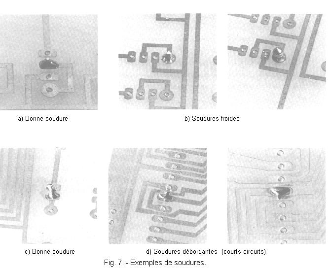
A good solder must look bright, smooth and silvery. The copper patch on the circuit board and the component terminal must form a single block as shown in Figure 7-a).
If, on the other hand, the weld has an irregular and granular appearance, or appears as a mercury ball (Figure 7-b), it is a cold weld due to the incomplete fusion of tin on the parts to to assemble. This is caused either by a too low temperature of the failure of the iron, or by a bad application of the failure on the elements to be welded not allowing the diffusion of the heat. It is possible to remedy a cold junction, by heating again and bringing, if necessary, a little welding and making sure that it diffuses well.
In any case, remember that for each solder, it is advisable to use a correct amount of tin taking the maximum of precautions so that it does not overflow on a pellet or an adjacent unrelated track thus creating a short-circuit as shown in Figure 7-d.
Protective varnish covering copper tracks that do not have to be welded should prevent this possibility, which is not excluded, however, and may occur due to unavoidable manufacturing tolerances.
In Figure 7-c, we can see how a good weld is produced, the execution of which requires special attention because of the presence of two copper tracks next to the weld point and which must remain isolated.
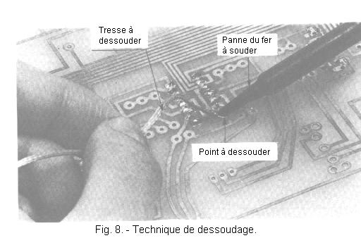
If, by excess of tin, you find yourself in one of the cases shown in Figure 7-d, it would be necessary to eliminate this excess solder which overflows the pellet by using the braid to desolder.
In Figure 8, we can see how this operation is performed : the braid is placed on the tin to be removed, and pressing the tip of the tip of the soldering iron on the braid, it heats up, melt the tin it absorbs. It is often necessary to resume the weld in question by avoiding this time to overflow.
Before beginning work, remember the need to proceed with the utmost care and care during the planned work phases, due to the complexity (although progressive) of the circuits to be carried out and the use of miniaturized components.
So, before you start editing, you must always read carefully all phases of the work without neglecting any, you can then proceed to the execution of each of the operations indicated by scrupulously respecting the instructions given.
In each case, avoid going to the next experiment until you have completed the previous one to completion.
By following these tips, you will ensure maximum success in carrying out your practical work and you will make the most of these experiences.


 The logic simulator
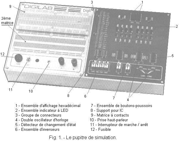
 click here for the next lesson or in the summary provided for this purpose.
 Top of page
 Next Page