Transmission of 8 Different Signals on a Single Driver Using a Multiplexer and a Demultiplexer :
9. - EIGHTH EXPERIMENT : EXAMINATION OF
A MULTIPLEXER WITH EIGHT WAYS
In the previous experiment, we have seen how it is possible to send two digital signals to a single driver using a two-input digital switch. This circuit is generally called a multiplexer.
The switching technique of digital electronic signals is very important and finds many applications.
Naturally, it becomes necessary to have more powerful multiplexers than the one with two inputs ; Four, eight, and sixteen-way integrated circuits are then used.
In this experiment, you will examine an eight ways multiplexer. This circuit, whose block diagram is illustrated in Figure 25, is also called multiplexer 8 to 1 because it has eight switchable inputs to an output.
It is obvious that it is necessary to indicate to the multiplexer which of the eight inputs must be "connected" to the output. This is done by means of three command entries. The binary number applied to these inputs indicates the selected input.
For this, each input is assigned a number between 0 and 7. It is sufficient to apply to the control inputs the binary number corresponding to the input selected for it to be switched to the output.
For example, entry 5 is selected with number 101, entry 6 with number 110, and so on ...
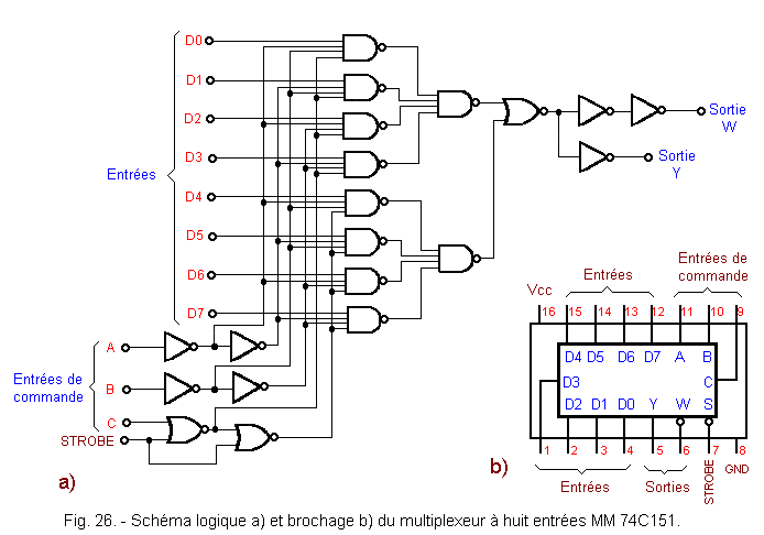
The integrated circuit that has these characteristics is the MM 74C151.
By observing its diagram shown in Figure 26-a, it is noted that it has eight entries denoted from D0 to D7 and three command entries denoted A, B and C.
The outputs are two in number : W and Y ; they are complementary to each other.
The STROBE input has the function of prohibiting any connection between any of the inputs and the output, when it is at the level H.
The pinout of the integrated circuit MM 74C151 is given in Figure 26-b.
9. 1. - REALIZATION OF THE CIRCUIT
a) Remove from the matrix the integrated circuits and links related to the previous experiment.
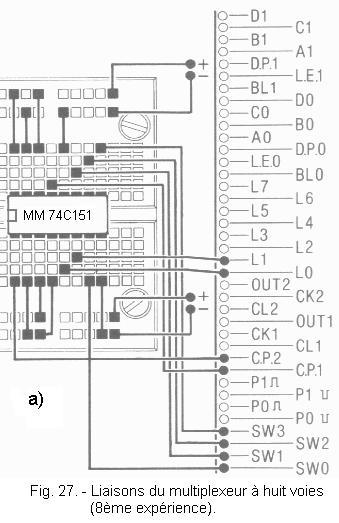
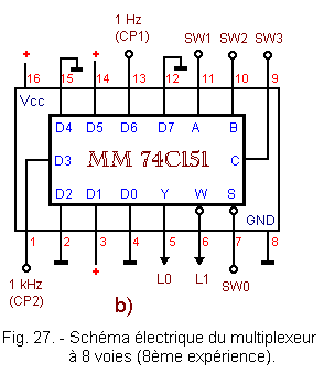
b) Insert on the matrix the integrated circuit MM 74C151 in the position shown in Figure 27-a and make the related connections.
The electrical diagram of the realized circuit is given in Figure 27-b.
The signals shown in the following table are applied to the eight inputs of the multiplexer.
Inputs
Signals
D0
L (0V)
D1
H (+ Vcc)
D2
L (0V)
D3
1 kHz
D4
L (0V)
D5
H (+ Vcc)
D6
1 Hz
D7
L (0V)
9. 2. - OPERATING TESTS
a) Switch SW0 to position 1 : you apply a level H to the input STROBE.
b) Apply power and observe the LEDs : L1 is on and L0 is off.
c) Switch the three switches SW1, SW2 and SW3 to any position : the state of the LEDs does not change.
Indeed, the STROBE input being at the level H, the output Y is permanently blocked at the level L and the output W at the level H. In other words, the multiplexer is inhibited.
d) Put SW0 on position 0 : you thus validate the multiplexer.
e) Switch switches SW1, SW2 and SW3 to position 0 ; this way, you apply the combination 000 to the control inputs, which selects the D0 input.
Now observe the LEDs : L0 is off and L1 is on. in fact, D0 is connected to ground (low level) and this low level is found at output Y.
f) Switch SW1 to 1 : now you apply the combination 001 on the control inputs and the input D1, connected to the "+", is therefore selected.
You notice that L0 is on and L1 is off.
g) Switch SW1 to 0 and SW2 to 1 : so the combination 010 is applied to the control inputs.
Thus, the input D2, connected to ground, is selected. You notice that L0 is off and L1 is on.
h) Leave SW2 on position 1 and put SW1 also on 1 : you thus realize the combination of command 011. One thus selects the entry D3 which receives the signal of frequency of 1 kHz : L0 and L1 are both lit, but they have a lower brightness than normal ; in fact, they turn on and off a thousand times per second which the eye can not detect.
i) Switch SW1, SW2 to 0 and SW3 to 1. In this way, the signal applied to D4 (100) is transferred to the output, that is to say 0V : L0 is thus off and L1 is on.
j) Leave SW2 on 0 and SW3 on 1 and switch SW1 to 1. The output is connected to input D5 (101), so L0 is on and L1 off.
k) Leave SW3 on 1 and switch SW1 on 0 and SW2 on 1 : L0 and L1 flash alternately at the frequency of 1 Hz. Indeed, one selects the input D6 (110) to which is applied the clock signal CP1 of 1 Hz.
l) Leave SW2 and SW3 on 1 and switch SW1 to 1 : you thus select the last D7 input (111) ; you notice that L0 is off and L1 is lit, which means that the level L present on input D7 is transferred to output Y.
m) Turn off the Digilab.
With this experiment, you have checked how by acting on the control inputs of a multiplexer, it is possible to switch on a single output, one of the signals present on eight inputs and how with the control input STROBE, we can validate or not the circuit.
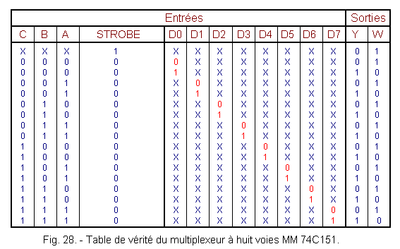
The operation of the multiplexer which we have just examined is summarized in the truth table of Figure 28.
The symbol X indicates that the logical state of the input concerned can be indifferently of 0 or 1 without the state of the outputs being modified.
For example in the first line, we find X on all inputs except a 1 for STROBE input. This means that when the STROBE input is in state 1, output Y is in state 0 and output W is in state 1 whatever the state of the other inputs.
10. - NINTH EXPERIMENT : TRANSMISSION
OF EIGHT DIFFERENT SIGNALS ON A SINGLE CONDUCTOR, USING A MULTIPLEXER AND A DEMULTIPLEXER
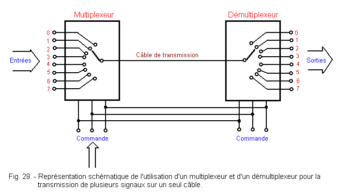
With the multiplexer of the previous experiment, eight different signals can be sent on a single output. This feature can be exploited to use a single cable when transmitting multiple signals. Naturally, at the other end of the cable, it is necessary to have a symmetrical circuit which directs the received signals towards eight lines.
This circuit is called demultiplexer ; it has a single input and several outputs (eight in the block diagram shown in Figure 29).
With this principle, it becomes possible to reduce the total length of the cables to use.
If, for example, the distance between the transmission point and the receiving point is 10 m and eight different cables are used (one per signal), 10 x 8 = 80 m of cable should be used.
With a multiplexer and a demultiplexer, however, only four cables (one for the signal and three for the control) are required, for a total of 10 x 4 = 40 m.
The saving is therefore 50%.
The economy is even greater when the number of signals to be transmitted is greater and when we adopt more complex transmission techniques that even save the cables transmitting the control signals.
The multiplexer having been examined previously, let us now turn to the examination of a demultiplexer.
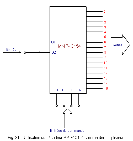
For this purpose, you will use an integrated circuit that you have already used as a decoder : the MM 74C154. The latter, used by exploiting the validation inputs, can also function as a demultiplexer.
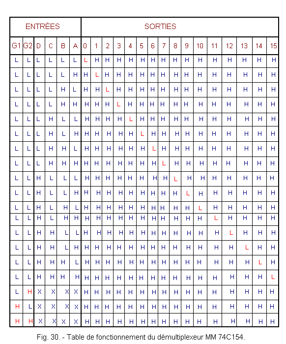
Consider its operating table shown in Figure 30.
Inputs G1 and G2 are validation inputs analogous to a STROBE input ; if only one of them is at level H, the decoder is blocked and all the outputs are at level H.
Suppose that the two inputs G1 and G2 are connected together and that they are used as a single input on which the signal of the line is applied. In addition, inputs A, B, C and D will be used as control inputs.
This is summarized in Figure 31.
By observing the truth table, it can be seen that if the inputs G1 and G2 are at the level L, one of the sixteen outputs is at the level L. It is the output which carries the number corresponding to the combination present on the inputs A, B, C and D.
If A, B, C, and D are at L, output 0 is selected because it is at L level.
If A is at level H and B, C, D at level L (combination corresponding to 0001), output 1 is selected and so on.
If, on the other hand, G1 and G2 are at level H, all the outputs are at level H.
It can therefore be concluded that the level present on the inputs G1 and G2 is found on the output selected by the control inputs A, B, C, D. This will be at the high level if G1 and G2 are at the High level or Low level if G1 and G2 are low.
Thus, the signal applied to the input of the circuit is switched to the output selected by the control inputs.
Here, eight of the sixteen outputs available will be used since the transmission side multiplexer is eight-way. We will therefore keep the D command input low, so only the outputs between 0 and 7 will be selected.
10. 1. - REALIZATION OF THE CIRCUIT
a) Leave the integrated circuit MM 74C151 on the matrix and remove all the links of the previous experiment.
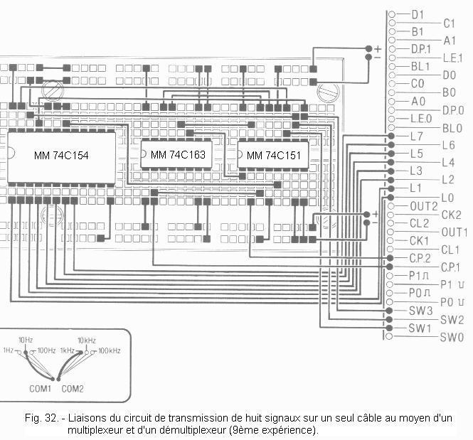
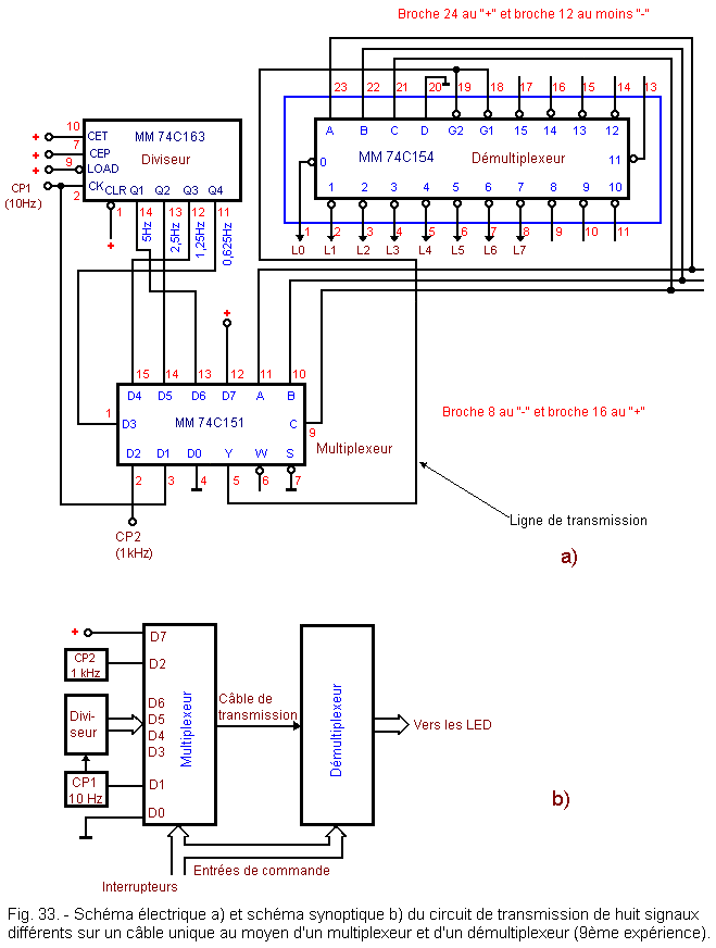
b) Insert the integrated circuits MM 74C163 (modulo counter 16) and MM 74C154 (demultiplexer) in the position indicated in Figure 32 and make the related connections. The circuit diagram of the realized circuit is given in Figure 33-a.
The counter, which is used as a frequency divider, is used to generate four rectangular signals of different frequencies (5 Hz, 2.5 Hz, 1.25 Hz and 0.625 Hz).
The block diagram of the realized circuit is shown in Figure 33-b.
At the inputs of the multiplexer are applied six rectangular signals of different frequencies generated by the two clock generators and by the divider.
The signals present at the inputs of the multiplexer are highlighted in the table of Figure 34.
Fig. 34. - Table of signals present at the inputs of the multiplexer.
Inputs
Broches
Sources
Signals
D0
4
-
0V
D1
3
CP1
10 Hz
D2
2
CP2
1 kHz
D3
1
Diviseur
(Q4, broche 11)
0,625 Hz
D4
15
Diviseur
(Q3, broche 12)
1,25 Hz
D5
14
Diviseur
(Q2, broche 13)
2,5 Hz
D6
13
Diviseur
(Q1, broche 14)
5 Hz
D7
12
+
5 V
The output Y of the multiplexer is connected to inputs G1 and G2 of the demultiplexer. The three switches SW1, SW2 and SW3 simultaneously control the multiplexer and the demultiplexer so that each of the signals applied to the inputs of the multiplexer is found on the corresponding output of the demultiplexer.
10. 2. - OPERATING TESTS
a) Put SW1, SW2 and SW3 on position 0.
b) turn on the Digilab and observe the LEDs : they are all lit except L0.
c) By switching the switches, make all possible combinations on the control inputs and observe each time the LED status : you must obtain the results shown in the table below.
SW3
SW2
SW1
L0
L1
L2
L3
L4
L5
L6
L7
0
0
0
0
1
1
1
1
1
1
1
0
0
1
1
10 Hz
1
1
1
1
1
1
0
1
0
1
1
1 kHz
1
1
1
1
1
0
1
1
1
1
1
0,625 Hz
1
1
1
1
1
0
0
1
1
1
1
1,25 Hz
1
1
1
1
0
1
1
1
1
1
1
2,5 Hz
1
1
1
1
0
1
1
1
1
1
1
5 Hz
1
1
1
1
1
1
1
1
1
1
1
1
Remember that the value 0 is indicated by an LED off, the value 1 by an LED lit and that each frequency value is displayed by means of an LED which turns on and off at the rate of this frequency.
This experience has allowed you to see how it is possible to control eight LEDs with eight different signals, using a single driver for these and three for control signals.
By dialing with the switches the binary number corresponding to a given input channel of the multiplexer, the signal present on the selected input channel is obtained on the corresponding output of the demultiplexer.
For example, with SW1 = 1, SW2 = SW3 = 0, the channel 1 (D1) of the multiplexer is selected, so the LED L1 flashes at the frequency of 10 Hz.
Of course, it is possible to apply to the demultiplexer control signals different from those of the multiplexer. In this case, it is possible to connect a transmission channel with a different reception channel ; for example, channel 1 can be directed to channel 5 and so on.


 Transmission of 8 different signals on a single driver using a multiplexer and a demultiplexer
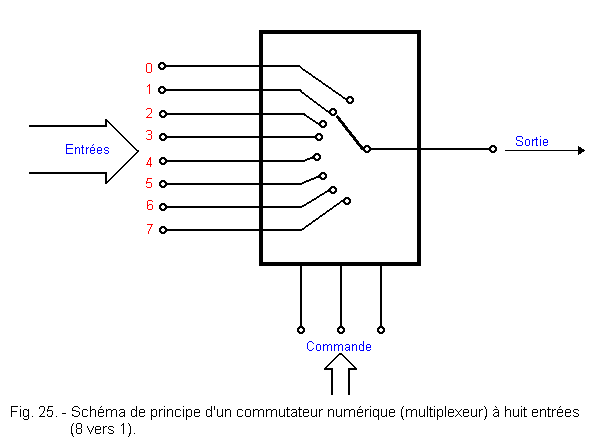
 Click here for the next lesson or in the summary provided for this purpose.
 Top of page
 Next Page