Associate with the N.P. junction previously described a material whose conductivity is of type N so that we obtain the following : N.P.N. (shown in Figure 7-a).
Junctions without polarization are not of great interest. In the case of Figure 7-a, there are several ways to organize this polarization. To tell the truth, only one interests us and we cut short by arranging it according to Figure 7-b.
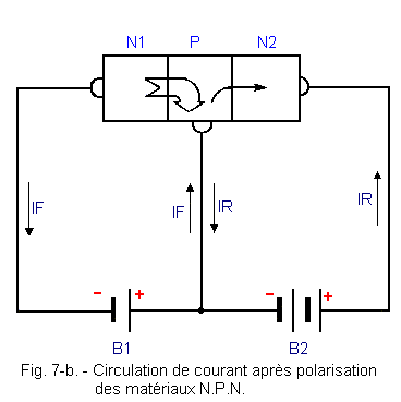
Starting from the left, the junction N1P is forward biased by the battery B1. Further to the right, the B2 cell polarizes the PN2 junction in the opposite direction.
What are the currents flowing in the external circuits connected to B1 and B2 ?
In that of B1, we find the presence of the electron flux of the majority carriers of the IF current.
The free electrons of the zone N1 flow into the zone P where they are picked up by the electrode connected to the + pole of the battery B1.
In the B2 circuit, only a minute current flows. It is due to the minority carriers of the PN2 junction which is polarized in reverse.
This current, remember, is due to the space charge (stack effect), created near the junction, by the presence of P-side anions (negative ions) and N2-side cations (positive ions).
The resulting electric field e favors the electron flow of the minority carriers from zone P to zone N2.
So far, this assembly is not a big interest. So something must be done to change that.
If the electrons of N1 are avoided, to recombine in the zone P and to leave by this place, they will be able to reinforce the current of electrons of the minority carriers caused by the polarization of B2.
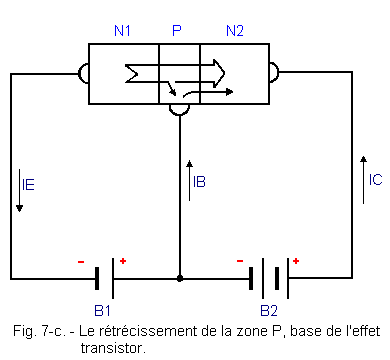
To arrive at this result, what artifice can we use ?
Not allowing the electrons time to recombine in the P zone and being subjected to the field e which will transfer them to the zone N2, implies a thickness of the zone P very weak.
Let's thin the P area as much as possible and reconsider the currents (Figure 7-c).
In the circuit of B1, no more current flows than a very weak current. On the other hand, we notice an important current in the circuit of B2.
The current of the majority carriers of N1 is transferred, in large part, in the zone N2 where it is attracted by the positive pole of B2.
Only a small part of this current flows in the circuit of B1. Some electrons have time to recombine in zone P and are attracted by the positive pole of B1.
It is interesting to note that the sum of the currents leaving the zones P and N2 is equal to the current injected into N1.
This description is what we call : the transistor effect.
It must be realized that this physical phenomenon is of paramount importance for the electronics because of the possibilities of miniaturization that it offers.
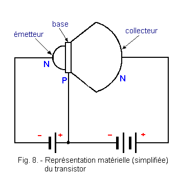
The sum of electrons collected in N2 and P is equal to that emitted by N1. We have just found a name for each of the electrodes connected to the N1 and N2 zones :
that of N1 will be called issuer
that of N2 that of collector.
The basis of all this path is based on the weak current leaving P. The electrode connected to this zone will bear the basic name.
Indeed, without the base current, there is no emitter current and, consequently, no collector current (with the exception of the reverse current of the PN2 junction).
Moreover, to further reduce the recombinations in the area P, so to improve the ratio between the collector current and that of the base current, this area will be less doped.
The latter having fewer holes, the recombinations will be smaller and the IC / IB ratio will be improved.
If the geometry of the zone N2 (the collector) is such that it allows a better collection of electrons, we will further improve this ratio (Figure 8).
The movements of the free electrons are not necessarily straight, if the surface of the collector is larger than that of the transmitter, the collection of electrons can only be favored. The transistor then takes on the appearance of Figure 8.
The size of the collector favors the collection of electrons (hence a better yield).
This type of junction transistor also takes the name of : bipolar transistor.
In Figure 7-c, we see that the collector current is composed as follows :
much of the transmitter current, about 0.9 times this one.
the reverse current of the PN2 junction, which is called ICBO (residual current collector-base).
On the other hand, the basic current consists of :
a small part of the emitter current
the ICBO current.
The base current thus consists of two currents in opposite directions.
We find that, using a low current base IB, under a low voltage B1 (direct polarization of the junction N1P), a large collector current IC is controlled at a voltage B2 higher than that of B1.
In summary :
With a very low power, we control a much higher power.
The transistor is a power amplifier.
It should be known that there are also other ways to organize the combination of N and P type materials.
Among others, that which leads to the transistor P.N.P. The explanation of the phenomenon is similar but, in this case, the doping taking the appearance of an injection of gaps or holes, it is reasoned by the displacement of these holes.
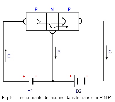
Figure 9 shows the hole currents in the P.N.P.
In reality, the current of electrons flows in the opposite direction (remember that if gaps move, it is because the electrons come to fill them).
We know that there are two types that result from the organization of materials N and P. These are :
transistors N.P.N.
transistors P.N.P.
These two families can be made of germanium or silicon. The latter is the most widespread material now for the manufacture of transistors.
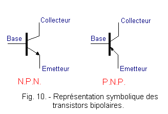
Figure 10 shows a frequent symbolization of these transistors.
This type of junction transistor also takes the name of : bipolar transistor.
In Figure 7-c, we see that the collector current is composed as follows :
much of the transmitter current, about 0.9 times this one
the reverse current of the PN2 junction, which is called ICBO (residual current collector-base).
On the other hand, the basic current consists of :
a small part of the emitter current
the ICBO current.
The base current thus consists of two currents in opposite directions.
We find that, using a low current base IB, under a low voltage B1 (direct polarization of the junction N1P), a large collector current IC is controlled at a voltage B2 higher than that of B1.
In summary :
With a very low power, we control a much higher power.
The transistor is a power amplifier.
It should be known that there are also other ways to organize the combination of N and P type materials.
Among others, that which leads to the transistor P.N.P. The explanation of the phenomenon is similar but, in this case, the doping taking the appearance of an injection of gaps or holes, it is reasoned by the displacement of these holes.
Figure 9 shows the hole currents in the P.N.P.
In reality, the current of electrons flows in the opposite direction (remember that if gaps move, it is because the electrons come to fill them).
4. - THE BIPOLAR TRANSISTOR (WE REPEAT THE SAME LESSON FROM THE DIAGRAMS)
We know that there are two types that result from the organization of materials N and P. These are :
transistors N.P.N.
transistors P.N.P.
These two families can be made of germanium or silicon. The latter is the most widespread material now for the manufacture of transistors.
Figure 10 shows a frequent symbolization of these transistors.
It can be seen that the transmitter is differentiated from the collector by an arrow.
This arrow does not represent the direction of circulation of the electrons, but the conventional direction of the electric current, that is to say the direction of movement of the holes. Care must be taken not to confuse these two ways of representing the flow of electrical charges.
For a standardization question, in schemas we have to use the conventional meaning.
The field of application of bipolar transistors extends from direct current to radio frequencies (U.H.F. : Ultra High Frequency).
The power dissipated on their collector ranges from a few hundred milliwatts to several hundred watts depending on the type.
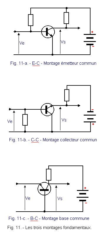
Depending on the destination of the assemblies, in which they intervene, we find three fundamental assemblies, allowing to use at best their characteristics and enumerated below :
common issuer
common collector
common base
Figure 11 symbolizes these three montages.
In the common transmitter, the input signal is applied between base and transmitter, the output signal is collected between collector and transmitter (the emitter electrode is common to both signals). This is the most common mounting, it provides between the input and output a power gain.
In the common collector arrangement, the input signal is applied between base and collector, the output signal is collected between emitter and collector. It allows to obtain a gain in current.
In the common base arrangement, the input signal is applied between transmitter and base, the output signal is collected between collector and base. It allows to obtain a voltage gain between the input and the output.
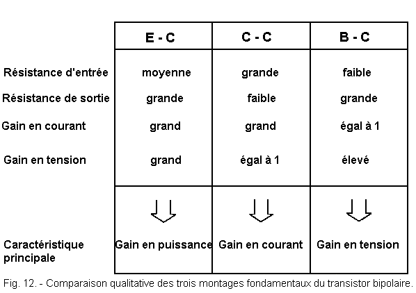
Figure 12 summarizes the main qualities of these three montages.
The main electrical quantities that characterize the transistor are four in number :
Two for the input circuit :
The basic current IB
The base-emitter voltage VBE
Two for the output circuit :
The collector current IC
The collector-emitter voltage VCE.
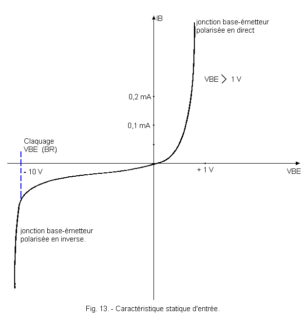
The two quantities relating to the input circuit correspond to the characteristic of a diode (base-emitter junction). Therefore, we find the polarization in the forward direction (to obtain a collector current) and the polarization in the opposite direction, with the avalanche phenomenon when this voltage becomes too high (Figure 13).
In general, this value is given by the manufacturer because it is destructive and must not be reached (VBE (BR)).
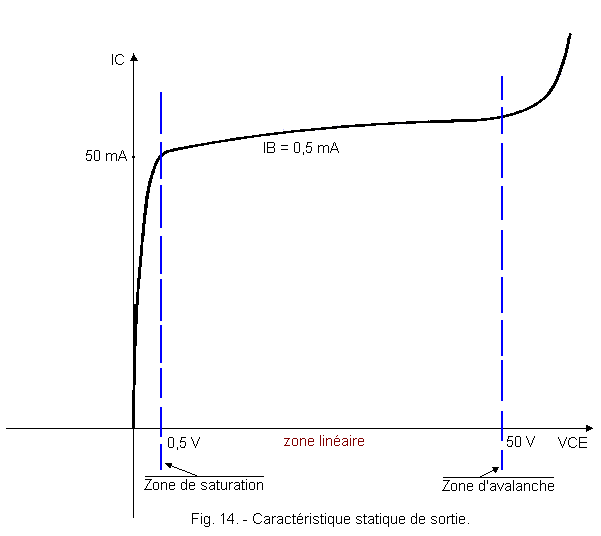
The output electrical quantities, collector current IC as a function of the collector-emitter voltage VCE, are read for different input currents IB.
This characteristic has three areas :
the saturation operating zone
the linear operating zone
the avalanche zone.
Figure 14 shows one of these characteristics.
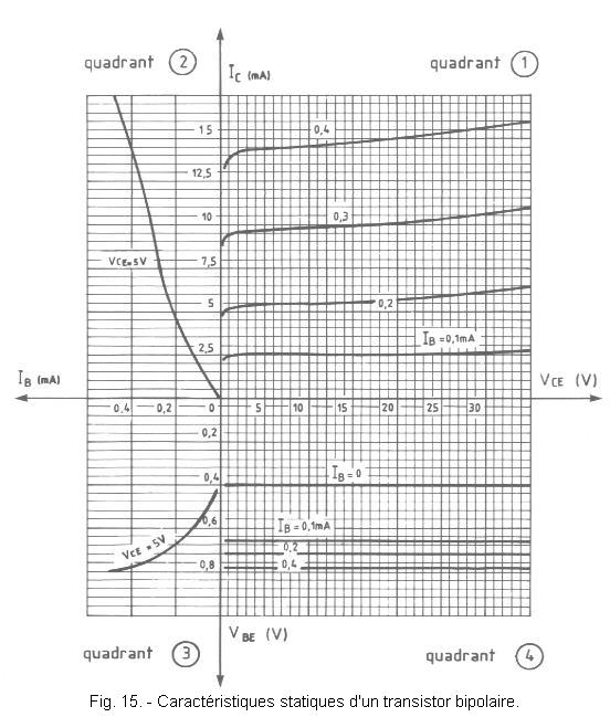
The static characteristics of the four-quadrant curve circuit transistor are shown in Figure 15, which gives an example.
Quadrant 1 of this figure represents the output characteristic : IC = VCE function for different values of IB. It makes it possible to determine the following elements :
the output resistance
the current gain
the charge line.
Quadrant 2 represents the direct transfer characteristic : IC = IB function. It allows the study of transistor behavior :
for weak signals
for strong signals.
Quadrant 3 represents the input static characteristic : VBE = IB function. It allows the study :
Differential input resistance
from the right of attack.
Quadrant 4 represents the inverse transfer characteristic : VBE = VCE function for different IB currents. This is the reaction coefficient of the output on the input.
A large number of parameters make it possible to define a transistor. Among these, we find the parameters h (hybrid parameters, derived from the matrix calculation).
These are the ones we use most frequently, so we will list them for guidance and remind you that these have been largely explained in the basic electronics lesson (see this lesson).
h11; it's from quadrant 3
It represents the input differential resistance :
h11 = DVBE
/ DIB
= re expressed in ohm
This ratio represents the value of the tangent to the characteristic drawn for the VCE
considered, with regard to the variations of VBE
and IB.
h12; it is taken from quadrant 4
et
and represents the reaction coefficient of the output on the input :
h12 = DVBE
/ DVCE
= µ
it is the relationship between two tensions, so without unity.
h21; it is taken from quadrant 2 and represents the direct transfer or gain in current :
h21 = DIC
/ DIB
= b ratio between two currents, therefore without unity.
h22; it is taken from quadrant 1 and represents the inverse of the output resistance or conductance :
h22 = DIC
/ DVCE
= 1 / rs expressed in siemens
In principle, the constructor gives the networks of quadrants 1 and 3.
The parameters h are often followed, as subscripts, by an E which affects these parameters at the transmitter-common assembly.
Example : h21E
= 100 pour IC = 5 mA.
This means that in the emitter-common circuit, this transistor has a current gain of 100
for an IC
of 5 mA, which corresponds to a base current of 0,05 mA.
To avoid cluttering this lesson, we will continue the procedure of bipolar transistors in saturated regime and in blocked mode corresponding to digital electronics ...


 The Bipolar Transistor
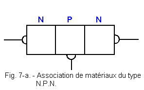
 Click here for the next lesson or in the summary provided for this purpose.
 Top of page
 Next Page