RS toggle with Validation Command - Toggle 74C74 :
5. - SECOND EXPERIENCE : EXAMINATION OF A ROCKET CIRCUIT R.S. WITH VALIDATION CONTROL
In the following exercise, you will add a command entry to validate the two inputs of the R.S. flip-flop. The command therefore allows the two logical levels to be taken into account on the inputs.
To realize this new circuit, you will proceed in the following way :
a) Disconnect the power supply and remove all previously established connections.
b) Make the new connections by referring to Figure 10-a and the following indications :
connect pin 1 of ICX with pin 11 of ICX
connect ICX pin 2 with ICX pin 6 and L1 contact of the connector group (use the triple conductor).
connect ICX pin 3 with ICX pin 4 and L0 contact of the connector group using the triple conductor.
connect pin 5 of ICX with pin 8 of ICX
connect pin 9 of ICX with contact SW1 of the group of connectors
connect pin 10 of ICX with pin 12 of ICX and with the contact P0
of the group of connectors (triple conductor)
connect pin 13 of ICX with contact SW0 of the connector group.
c) Insert the integrated circuit MM 74C00 into the ICX holder.
d) Put the two inverters SW0 and SW1 in position 0.
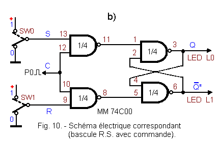
You have realized the illustrated circuit Figure 10-b. This circuit has three inputs R, S, C and two outputs Q and .
The inputs S and R are at the level L thanks to the switches SW0 and SW1. Input C is also at level L because the P0 button is released. Ultimately, this circuit is a RS flip-flop preceded by two NAND circuits whose operation depends on the C command.
e) Connect the power supply : one of the two LEDs lights up (L0 or L1) without it being possible to determine in advance which one.
f) Make the different combinations with the two switches SW0 and SW1. Note that there is no change of state on the outputs of the flip-flop.
g) Put SW1 on position 0 and SW0 on position 1. Press and hold the P0 button in this state. The input C passes to the level H and makes it possible to validate the two NAND by the pins 10 and 12. The two logical states on R and S are reversed on the two corresponding inputs of the rocker with the pins 1 and 5. The LED L0 turned on.
h) Release the P0 button : the LED L0 remains lit.
i) Now put SW0 in position 0 and SW1 in position 1. There is no change of state on both outputs.
j) Press and release the P0 button ; L0 goes out and L1 lights up.
k) Continue the experiment by testing the different combinations of SW0 and SW1 and observe both LEDs.
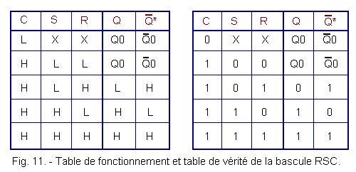
On the basis of the data obtained with these tests, you can establish the operating table and extract the truth table from the realized circuit, by adopting the procedure followed at the first experiment.
You can compare the results obtained with those reported in the two tables in Figure 11.
In these, the symbols X indicate that the inputs S and R can be indifferently at the level H or L (logical value 1 or 0) without influencing the state of the output of the circuit, that is to say without determining switching output levels when the C command is at level L.
You can see this result in practice by noting that if the P0 button is not pressed, the SW0 and SW1 switches can be switched to any position without determining a change of state of the LEDs.
On the other hand, if the P0 button is pressed, the state of the rocker depends on the levels present at the two inputs S and R.
In conclusion, you have been able through this experiment to see how it is possible to obtain an improvement of the R.S. flip-flop by the addition of two NAND circuits. This gives you a R.S.C flip-flop.
The characteristics of this rocker are the following :
using the input C, it is possible to control the operation of the rocker. More precisely, if the input C is at the level L, the flip-flop remains locked in the state where it is, independently of the variations of the levels applied to the inputs S and R. If the entry C is, on the other hand, at the level H, the flip-flop can switch and take a state depending on that of the inputs S and R.
If S and R are both at L, even if C is at H, the flip-flop does not change state. This configuration of the input levels corresponds to the idle state of the flip-flop.
If C is at level H, the entries are validated, that is to say that they have an action on the state of the rocker.
When S is at the level H and R at the level L, the latch takes the state 1, that is to say that the output Q is at the level H.
When S is at level L and R at level H, the flip-flop takes state 0, that is, output Q is at level L.
The advantage offered by the R.S.C flip-flop is as follows : the signals applied to the inputs S and R can cause a change of state of the flip-flop only when the authorization is given by the control input C.
Note that in this circuit, unlike that seen in the first experiment, the idle state is LL, S and R at the L level, and both inputs are active at the H level. This mode of operation is due to the inversion introduced by the first two NAND.
It is often necessary to memorize the logical state H or L of a signal at a given time by means of a control signal.
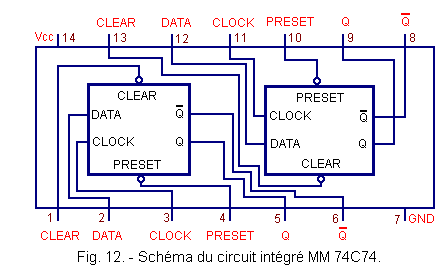
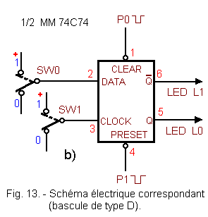
In this case, a D flip-flop of type MM 74C74 is used, the electrical diagram of which is given in Figure 12.
This integrated circuit, as you can see, comprises two identical D type flip-flops, only one of which will be examined.
As you can see in Figure 12, each D flip-flop has the following four inputs :
DATA : English term meaning "donnée" whose initial D gives the name to the rocker.
CLOCK : English term meaning "Horloge" ; it corresponds to the control input (input C of the latch relative to the previous experiment).
CLEAR :
term effacement
PRESET : term
predispose to state 1
You will see the function of these last two entries during the experiment.
In each of the two D flip-flops, there are two outputs Q and
which are complementary to one another.
Begin handling according to the following guidelines :
a) Disconnect the power supply and remove all connections made during the last experiment.
b) Remove the integrated circuit MM 74C00 from the ICX support and insert in it the integrated circuit MM 74C74.
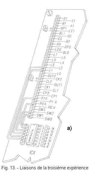
c) Make the connections shown in Figure 13-a and listed below :
pin 1 of the ICX support with the contact P0
pin 2
of ICX holder with SW0 contact
pin 3 of ICX holder with SW1 contact
pin 4
of ICX support with contact P1
pin 5
of ICX holder with L0 contact
pin 6
of the ICX holder with contact L1
d) Put SW0 and SW1 on position 0. With the connections made, you realized the circuit illustrated figure 13-b.
e) Connect the power supply and observe the L0 and L1 LEDs : one is lit and the other is off ; when the power is turned on, the rocker is positioned either in the high state or in the low state, without it being possible to predict which one.
You will now examine the functions of the DATA and CLOCK inputs, as the two CLEAR and PRESET entries are not considered at this time.
f) Set SW1 to position 1, setting the CLOCK input to H. You will see that the L0 LED is off, while L1 is on. This indicates that the Q output of the flip-flop was, if it was not already at the time of connection of the power supply, to state 0. The output Q is therefore at the level L and
au niveau H.
g) Now put SW1 on position 0 and place SW0 on position 1 : by observing the LEDs, you notice that the outputs have not changed state.
h) Set SW1 again to position 1 : you observe that L0 lights up immediately. This indicates that the flip-flop has entered state 1. It has memorized the fact that on the DATA input a level H (that is to say a logic level 1) is applied.
i) Perform the same operations several times, that is, switch the SW1 switch from position 0 to position 1 for the two positions of SW0.
You notice that every time SW1 goes from position 0 to position 1 (that is, from state 0 to state 1), the latch goes to the same state as that of the DATA input. Remember that the state of the flip-flop is defined by the state of the output Q and say that the flip-flop is in state 1 is equivalent to saying that Q is in state 1 or is in state H.
The flip-flop takes into account the level applied to the DATA input at the moment when SW1 is switched from state 0 to state 1.
j) Leave SW1 on position 1 and switch SW0 repeatedly. You notice that the state of the rocker indicated by L0 and L1 does not change. You have just seen that the flip-flop is sensitive at the DATA input only when the CLOCK input changes from level L to level H.
This is the fundamental characteristic of the D flip-flop. It has a control input like the RSC flip-flop seen in the previous experiment, but only switches at the time of the positive transition from the applied level to the control input, and not on a determined level applied to this entry. The input of the flip-flop is validated only during the very short time when the voltage level of the CLOCK input changes from level L to level H.
On the other hand, in the latch R.S.C., the entries are validated during all the time when the command is at the level H.
The CLOCK input is very important in digital circuits, because it allows them to operate in synchronism, that is to say that the changes of state outputs are made at the rate imposed by the clock.
In the next practices, the CLOCK function will be explained. For now, just consider it as a command entry validating the flip-flop.
Now let's take a look at the functions of the two remaining CLEAR and PRESET entries that have not been taken into consideration yet.
k) Press the P0 button to apply a pulse to the CLEAR input. You observe that L0 goes out and L1 ignites, regardless of the CLOCK input, which means that the flip-flop is forced to state 0.
l) Now press the P1 button, thus sending a pulse to the PRESET input. You observe that L0 lights while L1 goes out. The flip-flop is forced to state 1.
With these two tests, you have obtained the practical confirmation of the function of the inputs CLEAR and PRESET which, independently of the command input CLOCK, force the latch to one or the other of the two possible states at the output.
The term PRESET means "predispose", so this entry makes it possible to predispose the flip-flop to state 1.
The term CLEAR means "erase", so this entry allows, as you have seen, to erase any logical state 1 output of the flip-flop. It resets the output of the scale, (state = 0).
m) Finally, try to simultaneously level the two inputs CLEAR and PRESET while simultaneously pressing the two buttons P0 and P1.
You notice that the outputs Q and
pass both at the level L, while then releasing the buttons, the rocker goes to a state not being able to be determined in advance. This configuration of the two inputs is therefore of no practical use, just as in the flip-flop R.S., where the configuration of the entries = 0 and = 0 was not any more.
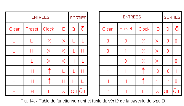
On the basis of the results obtained with the tests carried out, you can draw up the operating table and draw from it the truth table of the rocker D shown in Figure 14.
The operating table summarizes all the results of the experiment. The upward arrows in the column of the CLOCK entry represent a positive transition which is the transition from the L level to the H level of the signal applied to this input.
Remember also that the symbol X means that the input to which it refers, can be indifferently at the level L or H without influencing the state of the rocker with the conditions specified for the other entries.
From the experiment made and from the observation of the tables of Figure 14, one can summarize thus the operation of the flip-flop D :
the circuit stores the state of the DATA input at the time of the transition from the L level to the H level of the signal applied to the CLOCK input.
PRESET and CLEAR entries are not validated by the CLOCK entry. They are used to respectively position the circuit in state 1 or in state 0.
This is very useful when you connect the power supply, for example to put the flip-flop in the desired state, instead of letting it take an indeterminate state.
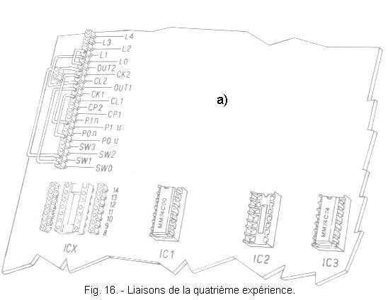
7. - FOURTH EXPERIENCE : USE OF A "ROCKET D" AS DETECTOR OF POSITIVE TRANSITIONS
In this experiment, you will check how it is possible to exploit the characteristics of the D flip-flop, adding to the digilab that you are building another circuit that will be particularly useful for later experiments.
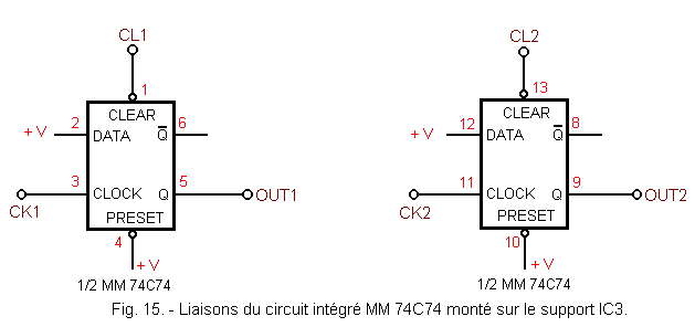
a) Disconnect the power supply, remove the integrated circuit MM 74C74 from the ICX holder and insert it into the IC3 holder.
Through the tracks of the printed circuit, the different pins of the integrated circuit are connected to the different contacts of the group of connectors as represented by the diagram of Figure 15.
Indeed, as you can see, the inputs CLEAR, CLOCK and the output Q of the first flip-flop are respectively connected to the contacts marked by the symbols CL1, CK1 and OUT1 of the group of connectors, while the same inputs and outputs of the second flip-flop are connected to contacts CL2, CK2 and OUT2.
The PRESET and DATA inputs are connected to the + V voltage and are therefore permanently at the H level, while the
output is not connected.
The PRESET input is connected to level H so that it does not influence the operation of the flip-flop.
The output
is not connected because it is not used.
b) Now make the connections between the different contacts of the connector group shown in Figure 16-a as listed below :
CK1
with SW0
CK2
with SW1
CL1
with P0
CL2
with P1
OUT1
with L0
OUT2
with L1
In this way SW0 and connected to the CLOCK input of the first flip-flop, the Q output to the L0 LED and the CLEAR input to the push-button P0.
The second flip-flop is connected in a similar way to the switch SW1, the LED L1 and the push-button P1.
Now do the following :
c) Connect the power supply and set SW0 and SW1 to the 0 position.
d) Press the P0 button, so you apply a negative impulse to the CLEAR input of the first flip-flop. You notice that L0 goes off, so that the rocker goes to state 0.
In this way, the circuit is pre-positioned or initialized, that is, it has been put into a known and desired state so as to be able to continue the experiment from a well-determined and chosen state, in this case the state 0.
e) Now switch SW0 to position 1. L0 comes on immediately. Indeed, on the input CLOCK is applied a transition from the level L to the level H, the rocker thus takes the state determined by the input DATA.
Since the latter is at the level H, the rocker goes to the corresponding state, that is to say at the level H thus causing the ignition of L0.
If the test did not provide the expected results, review the connections more closely and make a careful visual inspection of the PCB tracks connecting the IC3 bracket and the connector group contacts. Repeat the welding.
f) Put SW0 back on position 0 and then press the push-button P0. The LED goes out.
g) Try to switch SW0 several times from 0 to 1 and vice versa.
At each transition from state 0 to state 1 performed in this way, you will see that L0 lights up if it is not already on. Push-button P0 turns it off.
h) Repeat the same operations on the second flip-flop by pressing SW1 and push-button P1 and observing LED L1.
After handling, leave the integrated circuit MM 74C74 permanently inserted into the IC3 holder.
You have thus experimented with a circuit that detects the transitions from level L to level H : it will be particularly useful for detecting impulses that are too brief to be visualized by means of the LED. It can be said that the circuit memorizes the pulses by setting itself to the state 1 and remains in this state even after the disappearance of the pulse of which it indicates the existence.
In the next practice, you will examine other types of circuit and you will continue the experiments with circuits more and more complex.


 Examination of a D flip-flop
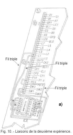
.gif)
 Click here for the next lesson or in the summary provided for this purpose.
 Top of page
 Next Page