With this manipulation, you will learn how to write in memory. This is possible because the memory we have and the type to read / write. There are, on the other hand, memories called ROM, in which it is not possible to write but only to read.
There is however a problem : they are the same terminals that allow reading and writing. It is therefore necessary to add to the assembly, as we will see, the bidirectional buffer TRI-STATE which was examined in the first experiment of this same practice 12, so that only the selected circuits remain in relation.
6. 1. - REALIZATION OF THE ASSEMBLY
a) Leave the assembly unchanged. Insert the integrated circuit 74LS245 (bidirectional buffer TRI-STATE) into the array in the position shown in Figure 33.
b) Make the links shown in Figure 33 on the matrix without removing the existing ones.
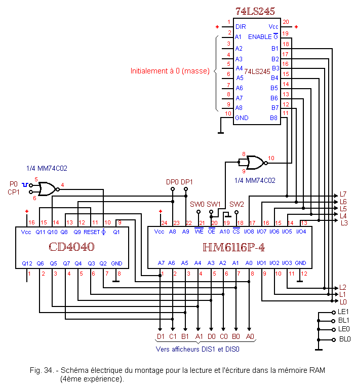
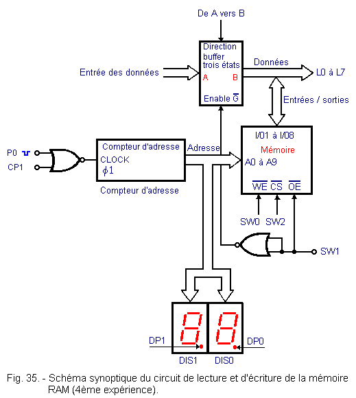
In Figure 34 and Figure 35 are respectively represented the electrical diagram and the block diagram of the realized circuit.
A buffer has been added for its TRI-STATE characteristic. Thus, the data entry remains separate from the output as you will see during the experiment.
6. 2. - OPERATING TEST
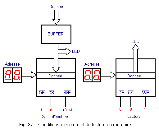
a) Put SW0 on position 1 (reading).
b) Put SW1 on position 0 ; in this way, the output of the memory is validated (by means of )
and the buffer is inhibited. The outputs of the latter are isolated because they are in the "high impedance" state.
c) Put SW2 on position 0 ; the memory is thus validated.
d) Turn on the Digilab.
e) By the method described in the previous experiment, read some of the memory positions. Once again, you find random values.
f) Now put SW1 on position 1 ; thus, the output of the memory is inhibited and the buffer validated :the LEDs are all off.
Indeed, the buffer is positioned to transmit from A to B and all A inputs are connected to the ground.
The same data going to the LEDs appears at terminals I / O1 to I / O8 of the memory as input data.
g) Set the memory to address zero using the method adopted in the third experiment : the two decimal points DP1 and DP0 must be off, DIS0 and DIS1 indicate 00.
h) Put SW0 on the 0 position corresponding to the writing.
i) Put SW0 on position 1 : in this way, entry
goes from state 1 to state 0 and then back to state 1. You have thus completed a write cycle.
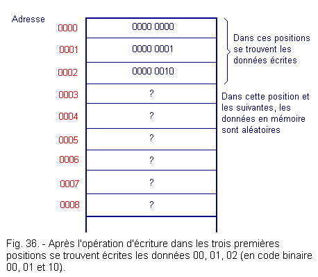
In the position indicated by the address (in our case, position 0000) is written the data present on the entries that is to say 0016.
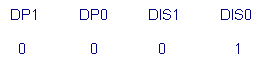
j) Now move the address counter (clock on 1 Hz frequency) by one unit by pressing the P0 button. The indication of the displays is as follows :
It corresponds to the address 0001.
Suppose that at this address we want to write the hexadecimal value 01. It is necessary to compose it at the input of the buffer, by proceeding as follows :
k) Without turning off the power, move the link from pin 2 of the buffer (corresponding to A1) to the ground, connecting it to the positive voltage instead of the ground ;LED L0 lights up.
l) Then perform a write cycle, setting SW0 to position 0 and then to position 1 again.
m) Write to address 0002 the decimal value 02 which is written in binary code 10. To do this, connect pin 2 of the buffer back to ground and pin 3 (A2) to the positive voltage : LED L1 lights. Then perform a write cycle.
We have now written to the first three addresses of memory (Figure 36). Check that the data has actually been recorded, by performing a read cycle as shown below.
n) Set the address to 0000 and set SW1 to 0, so that the buffer is disconnected and the output of the memory is validated ; the value contained in the first memory position can be read on the LEDs. Since we wrote 00, all LEDs are off.
o) Now read the value in the second position. To do this, simply increment the address of 1 : we get 0001 ; you must then read the value 01.
p) Then examine the following position : you must read the value 02 (10 in binary code).
q) Following the procedure described, practice writing and reading data in memory, remembering that you should not turn off the power during these operations, so as not to erase the data already written.
r) At the end of the tests, turn off the Digilab.
Let's summarize the procedure for writing to memory:
We select the address.
We position the data on the input of the buffer.
Data output is inhibited by setting SW1 to position 1.
We put SW0 on position 1.
We validate the entire memory by switching SW2 to the 0 position.
One cycle is carried out with SW0 by putting it on position 0 then again on position 1.
In Figure 37 are schematized the operations of writing and reading.
As you noted, at power up, the memory contains random data. It may be useful for some applications to reset all memory positions. This operation is called memory erase or reset.
One could proceed as in the fourth experiment by writing the data 00 to each address with a single write cycle.
However, although this memory is not synchronous input (
valid on a level and not on a front), we will consider that read and write are validated on a front in order to use a general method that we will useful later. It is this automatic method that will be described during this experiment.
7. 1. - REALIZATION OF THE CIRCUIT
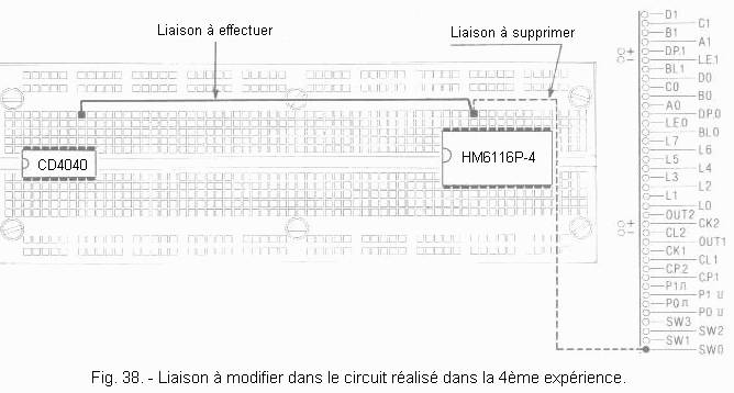
Keep all the links made in the previous edit.
Remove only the link that connects SW0 to pin 21 of the memory and connect it to pin 10 of the CD4040 counter.
Then make sure that all the buffer entries are connected to the ground.
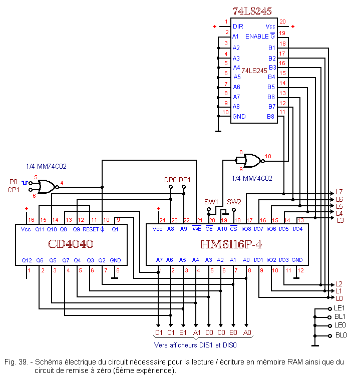
Figure 38 shows the new link and Figure 39 shows the resulting electrical schematic.
The clock signal which increments the counter goes in this way to control the read / write through .
7. 2. - OPERATING TEST
a) Put SW1 on position 1 : in this way, the output of the memory is inhibited. The buffer is validated.
b) Put SW2 on position 0 : the memory is thus validated.
c) Turn on the Digilab : the LEDs are all off because the data present at the buffer input is at 00. The displays indicate any address.
d) Press and hold P0 : the address is incremented and, at the same time, in the corresponding memory position the information 00 is written.
e) When the meter has completed a cycle and returned to the starting address, release P0 ; all memory has been reset.
f) Check that the memory actually contains 00 at each position, reading the contents as follows :
Without turning off the power supply, disconnect pin 10 from the CD4040 from the pin 21 connection and connect it again to SW0.
Set SW0 to position 1, allowing you to read the memory.
Set SW1 to 0, thus enabling the output of data from the memory.
Observe the LEDs ; they are all extinct.
By pressing P0, scroll through the addresses and make sure that the LEDs remain off : this will confirm that the memory contains only zeros, so it has been erased.
g) At the end of the test, switch off the Digilab.
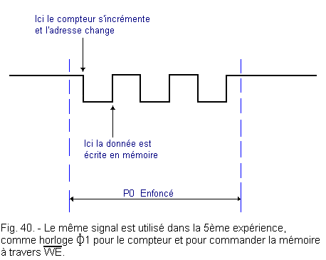
In summary, the memory could be reset by using the clock signal from the contact CP1. You may notice that the counter is incremented on the falling edge of the rectangular signal while during the same time, the memory records the data on the rising edge as seen in Figure 40.


 Clearing Memory
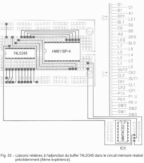
 Click here for the next lesson or in the summary provided for this purpose.
 Top of page
 Next Page