Study of a 12 stages CD4040 Counter and a 74LS245 Bidirectional Buffer :
2. - PREPARATION OF HARDWARE
To carry out the experiments planned in this practice, you will need to use the following equipment :
1 integrated circuit MM 74C163
1 integrated circuit MM 74C193
1 integrated circuit MM 74C02
1 integrated circuit HM 6116P-4
1 integrated circuit 74LS245
1 integrated circuit CD4040
3. - FIRST EXPERIENCE : EXAMINATION AND TEST OF OPERATION OF A BIDIRECTIONAL BUFFER THREE STATES.
In this experiment, the integrated circuit 74LS245 will be used, it contains eight bidirectional buffers TRI-STATE, as shown in the diagram of Figure 14.
At terminals 2, 3, 4, 5, 6, 7, 8 and 9 can be connected eight lines from A1 to A8, and eight others can be connected to pins 18, 17, 16, 15, 14, 13, 12 and 11 from B1 to B8.
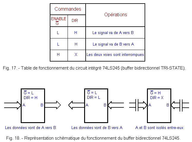
The data can be transmitted from A to B or from B to A depending on the state of the command applied to the "DIR" pin (abbreviation of direction) when the ENABLE command entry
is at the low level.
When the entry ENABLE
is high, the passage of the data is prohibited in both directions, because all the buffers internal to the integrated circuit are in the state "high impedance", which is equivalent to say that the outputs from these are disconnected from the bus.
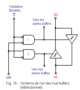
You can notice the sign represented inside each buffer ; it indicates that the buffers used comprise a fitness circuit Schmitt trigger type.
You can see Figure 15, the internal configuration of the circuit for only one of the eight channels A to B or vice versa ; we will use this diagram later to understand the circuit and establish the operating table during the experiment.
Finally, note that the 74LS245 circuit is a T.T.L. and for this reason, it must be powered with a stable voltage of 5 V. Higher voltage could damage it.
3. 1. - REALIZATION OF THE CIRCUIT
a) Remove from the contact matrix all the connections and components related to the last experiment.
b) Ensure the correct position of the Digilab on-off switch. It must be in the OFF position when connected to the mains.
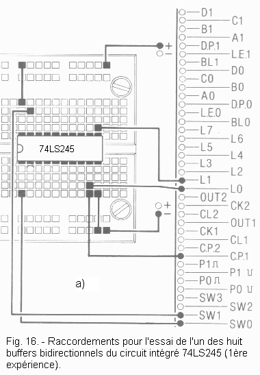
c) Insert the 74LS245 Integrated Circuit into the matrix in the position shown in Figure 16-a. Then make the necessary connections.
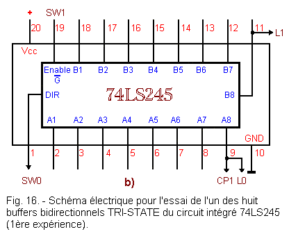
Figure 16-b shows the diagram of the electrical circuit made.
3. 2. - OPERATING TEST
In this first phase, you will check the operation of one of the eight bi-directional buffers of the integrated circuit.
a) Put SW1 on position 0 to validate the circuit and put SW0 on position 1.
b) Switch
on the Digilab : L0 and L1 then flash at a rate of 10 Hz. When SW0 is in position 1, the passage of the signal in the direction of A8 to B8 is allowed. This is because the output of the gate 2of the
Figure 15 is high while that of the gate 1 is low thus prohibiting the direction B8 to A8.
c) Put SW1 on position 1 ; in this way, both channels are cut off and the signal does not go in either direction.
Indeed, L0 flashes again, controlled by the signal from CP1 ; on the other hand L1 does not blink anymore. It has a lower brightness than normal.
d) Without changing the other links, connect the output B8 of the buffer (pin 11) with the +: L1 lights up with full intensity.
e) Connect output B8 to ground : L1 goes out. You have thus found that L1 can be controlled independently of the buffer which, not validated, does not intervene.
f) Remove the connection between pin 11 of the buffer and the mass.
g) Turn off the Digilab.
Now reverse the direction of transmission, applying the rectangular signal supplied by CP1 to input B8. Observe what's happening on A8.
h) To do this, remove the connection between pin 9 and contact CP1, then connect pin 11 and contact CP1. Then switch SW1 to the 0 position to validate the circuit again.
i) Set SW0 to 0, thus reversing the direction of transmission from the previous test.
j) Switch on the Digilab ; you see that L1 and L0 are both flashing, the signal goes from B8 to A8. To check if the signal is actually going from B8 to A8, repeat the same procedure as for the previous case.
k) Set SW1 to position 1 : both channels are interrupted, L1 flashes, while L0 remains lit.
l) Connect L0 with the +; you notice that it lights up.
m) Put L0 to the ground ; it goes out.
You have just checked the two directions of signal transmission between A8 and B8 of one of the eight channels of the integrated circuit. Follow the same procedure for the other seven channels to verify proper operation.
n) Turn off the Digilab.
Based on the results obtained, you can build the operating table of the bidirectional buffer shown in Figure 17 which can be summarized schematically in Figure 18.
4. - SECOND EXPERIENCE : OPERATING TEST OF A TWELVE STAGE COUNTER.
To perform the following experiments, it will be necessary to use a counter. In previous practices, you experimented with different types of meters ; the one you are going to examine now is no different from the others in terms of its design, but it has the great advantage of containing 12 floors in a single integrated circuit.
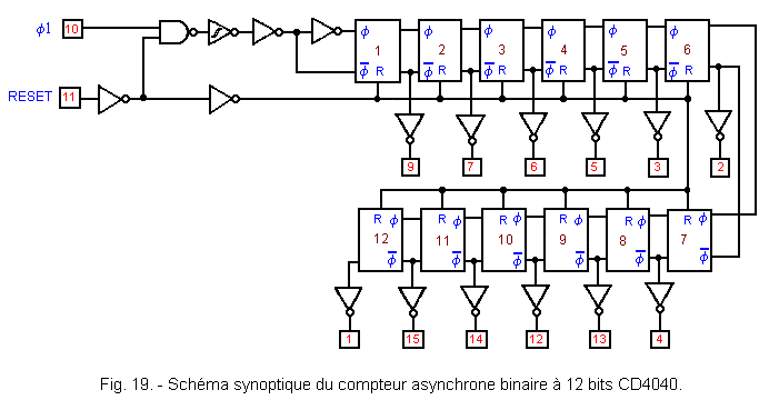
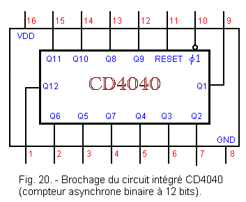
This is the CD4040, bit asynchronous counter 12 bits, whose block diagram is shown in Figure 19. The pinout of this circuit is shown in Figure 20.
The pulses to be counted must be applied to the input indicated by f1, which is connected to a NAND gate controlled by the RESET input.
The NAND gateway is followed by a Schmitt trigger that serves to improve the quality of the signal, then come two inverters that drive the divider chain.
The counter is incremented each time the input f1 goes from the high level to the low level, that is to say to each falling edge. This is symbolized by a bubble placed on the input f1 in Figure 20.
The RESET input resets the counter to zero, it is asynchronous ; as soon as a level H is applied to it, the counter goes to 0.
The counter can range from 0 to 4095 (212 positions). On the outputs, the binary number is obtained by applying the positive logic convention (level L = 0, level H = 1).
4. 1. - REALIZATION OF THE CIRCUIT
a) Remove from the matrix the links and components related to the previous experiment.
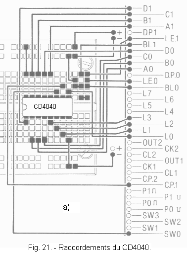
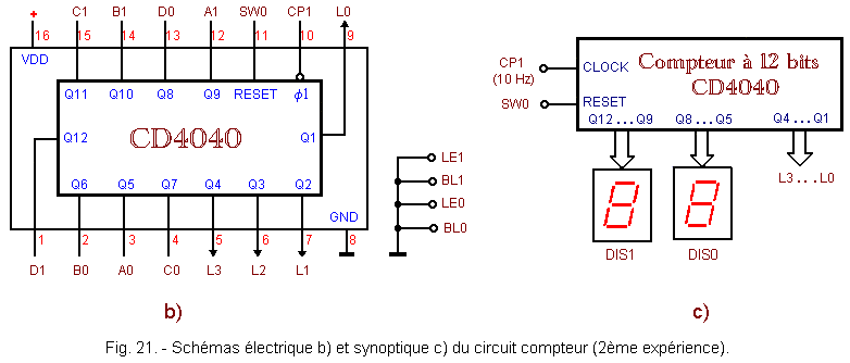
b) Insert the integrated circuit CD4040 into the matrix in the position indicated in Figure 21-a and make the connections.
The electrical diagram of the realized circuit is shown in Figure 21-b, while Figure 21-c shows its block diagram.
4. 2. - OPERATING TEST
a) Put SW0 on position 1.
b) Connect the power supply : you observe that the LEDs of L0 to L3 are off and that the two displays indicate the digits 00.
c) Put SW0 on position 0 : you notice that the counter is unlocked and starts counting from 0.
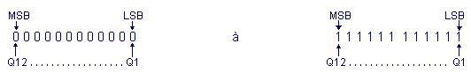
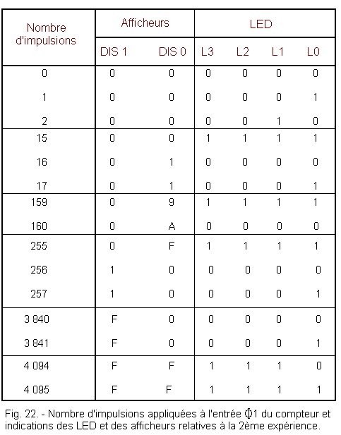
On the twelve outputs of Q1 to Q12, there is a binary number of twelve bits ranging from :
The most significant bit (M.S.B.) corresponds to the output Q12 and the least significant bit (L.S.B.) to the output Q1.
With the LEDs L0 to L3, the bits of Q1 to Q4 are displayed, with DIS 0, the bits of Q5 to Q8 can be displayed and with DIS 1, those of Q9 to Q12 are displayed.
Observe LEDs and displays ; since the clock is at the frequency of 10 Hz, the LED L0 flashes at the frequency of 5 Hz, L1 at the frequency of 2.5 Hz, L2 at 1.25 Hz, L3 at 0.625 Hz.
After the sixteenth clock pulse, the incrementation of the indication of the displays starts, the latter being in hexadecimal code, from 00 to finish at FF at the end of the count.
When observing the LEDs and displays, check the correct operation of the meter by referring to the table in Figure 22. The number 0 in the column should match the LED off and the number 1 with the LED on.
Of course, it is not a matter of counting the clock pulses up to 4095 to check the table : it suffices to observe that the LEDs and the displays follow the sequence indicated in the table.
d) After completing the test, turn off the Digilab.
By commenting on the experiment, it can be said that each stage of the counter divides the frequency of the signal applied to its input by two ; if the signal is injected at 10 Hz, coming from the contact CP1, at the input f1 of the counter, at the different outputs, signals are obtained whose frequency is each time reduced by half. This can be easily checked by observing the rate at which the LEDs are flashing and at which the displays are incremented. The table in Figure 23 shows the frequency and the period of the signals of the different stages of the meter and summarizes the results of the test.
Fig. 23. - Frequency in Hz and corresponding period in seconds of the signals obtained at the outputs of the counter during the 2nd experiment.
Output
Pinout
Frequency (Hz)
Périod (s)
Q1
9
5
0,2
Q2
7
2,5
0,4
Q3
6
1,25
0,8
Q4
5
0,625
1,6
Q5
3
0,3125
3,2
Q6
2
0,15625
6,4
Q7
4
0,078125
12,8
Q8
13
0,0390625
25,6
Q9
12
0,0195313
51,2
Q10
14
0,0097656
102,4
Q11
15
0,0048828
204,8
Q12
1
0,0024414
409,6
As you can see, the frequencies range from 5 Hz to 0.0024414 Hz, which is an extremely low frequency. So just a little attention to observe the phenomenon and in case there are still some obscure points, do not hesitate to repeat the experience several times.


 Functional test of a 12 stages Counter
.gif)
.gif)
.gif)
 Click here for the next lesson or in the summary provided for this purpose
 Top of page
 Next Page