Description of TIL 311 Displays and Operation Control :
5. - MOUNTING TWO HEXADECIMAL DISPLAYS ON THE DIGILAB
To complete the assembly of the circuit board on the digilab, you have to mount both DIS0 and DIS1 displays, as well as control circuits of decimal points.
The Figure 9 shows the completed assembly.
These two displays will read numbers much easier.
Indeed, it is easier to read a hexadecimal or decimal number than a binary number.
You learned that the hexadecimal code is Base 16 and that the sixteen characters used include the ten decimal digits (From 0 to 9) and the six letters from A to F.
These six letters correspond to the decimal numbers from 10 to 15.
The Figure 10 shows the conversion table between the binary, decimal and hexadecimal codes for the first sixteen decimal numbers.
Fig. 10. - Conversion table of the first 16 decimal numbers in binary and hexadecimal code.
Number
Decimal
Binary
Hexadecimal
Zero
0
0000
0
One
1
0001
1
Two
2
0010
2
Three
3
0011
3
Four
4
0100
4
Five
5
0101
5
Six
6
0110
6
Seven
7
0111
7
Eight
8
1000
8
New
9
1001
9
Ten
10
1010
A
Eleven
11
1011
B
Twelve
12
1100
C
Thirteen
13
1101
D
Fourteen
14
1110
E
Fifteen
15
1111
F
A binary number can be immediately converted into a hexadecimal number by grouping by four the bits of this number and consulting the table of Figure 10.
Example :
Conversely, hexadecimal-to-binary conversion is :
The transition from hexadecimal code to decimal code is slower.
In general, you have to go through the binary code. It is also possible to operate as well :
A2F = (A x
162) + (2 x 161) + (F x 160) = (10 x 256) + (2
x 16) + (15 x 1) = 2560 + 32 + 15 = 260710
d) Take the two resistors R16 and R19 of 4700 Ω, 5% (yellow - purple - red - gold) and after having properly folded the terminals, place them on the circuit board at the place indicated by the corresponding symbol.
Then solder their terminals on the copper tracks and cut the excess parts.
e) In the same way, solder the two resistors R17 and R18 of 220 Ω, 5% (red - red - brown - gold).
f) Check transistors T8 and T9 of type BC 238 B or its equivalent. For this, use the ohmmeter and the method described in practice 2. Then arrange these two transistors at their location on the printed circuit, respecting the orientation of the three electrodes (the flat serves as a reference).
Weld the three electrodes and cut off the excess parts.
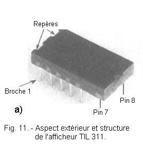
g) Take both displays and watch over them.
At one end, they have a semicircular notch ; at the other end, they have two semi-circular notches.
Figure 11 shows the different views of these displays, as well as the various landmarks.
The pins on the TIL 311 displays are fragile, so handle them carefully.
h) Insert the two TIL 311 displays at their location labeled DIS0 and DIS1 (see Figure 9), taking care to avoid bending the pins.
The two semi-circular notches are located towards the top of the printed circuit (the screen printing of it has only one) and the semicircular notch only is located towards the inscription DIS1 and DIS0 (towards the bottom ).
i) Check all welds made.
j) Reassemble the circuit board and the metal front on the digilab after connecting the three pins connector.
Before going to the functional check, describe the characteristics of the displays and the circuit that you have just mounted.
The box contains the actual display that allows viewing one of sixteen hexadecimal characters (from 0 to F) ; it also contains a decoder circuit with four inputs and finally, a circuit which makes it possible to memorize a hexadecimal character.
The hexadecimal character is formed from a matrix with twenty miniature LEDs as shown in Figure 11-b.
There are two other miniature LEDs that indicate decimal points or commas.
If you look through the box, you see a small rectangle that is the integrated circuit providing decoding and storage functions.
The technology of this integrated circuit is TTL type.
The case has five pins on one side and six on the other.
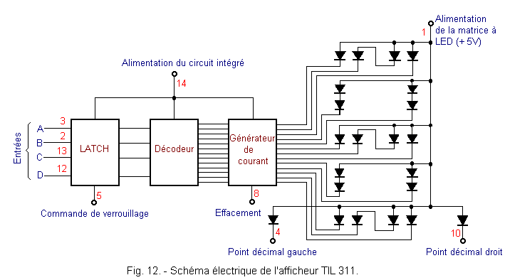
The electrical diagram of the display is shown in Figure 12.
The binary number is applied to the inputs A, B, C and D.
The number can be stored at the output of the LATCH block of the integrated circuit.
If the LATCH validation command (pin 5) is at L level, the LATCH outputs follow the levels present on the inputs.
The LATCH is in the "transparent" position.
On the other hand, if this command passes to level H, the data present at this moment on the inputs are memorized.
In other words, a variation in input data does not result in any change in the four LATCH outputs.
The four LATCH outputs arrive at the four decoder inputs.
This decoder has thirteen outputs for lighting the LEDs on the matrix.
A current generator is interposed between this decoder and the LED array.
This current generator provides a constant current that allows the LEDs to light up.
If the BLANKING command input is at level H, all twenty LEDs in the matrix are off.
The other two LEDs of the decimal points are not influenced by this command input.
The supply of the LED matrix may be different from that of the integrated circuit.
This can be advantageous because on the pin 1 of the housing, it is possible to apply a no stabilized voltage, which reduces the intensity of the current delivered by the stabilized voltage.
While the twenty LEDs of the matrix are controlled by an internal current generator, the two decimal points require an external current generator.
In this arrangement, only the two decimal points to the right of each display are used.
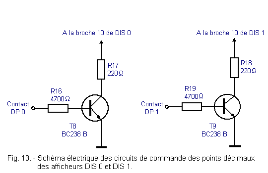
Their control is carried out using the circuit indicated in Figure 13.
For each circuit, the transistor provides a switch and current amplifier function.
If the contact DP0 is at the level L, the transistor T8 is blocked ; the LED in series with R17 is off.
If this same contact DP0 goes to level H, T8 becomes saturated and the corresponding LED lights up.
The operation is the same for T9.
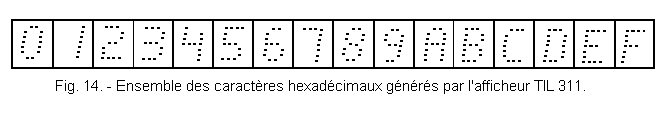
The Figure 14 shows all the characters that the display can generate. Each dot represents a lit LED.
The pins of each display are connected by means of the printed circuit to the contacts of the group of connectors.
The inputs A, B, C and D of each display are connected to the contacts A0, B0, C0 and D0 for the display DIS0 and A1, B1, C1 and D1 for the display DIS1.
The input for the right decimal point is connected to the DP0 contact for the DIS0 display and to the DP1 contact for the DIS1 display.
The blanking input is connected to the BL0 contact for the DIS0 display and to the BL1 contact for the DIS1 display.
The lock control input (LATCH) is connected to the LE0 contact for the DIS0 display and to the LE1 contact for the DIS1 display.
There are seven contacts for each display.
The power is applied directly through the printed circuit.
5. 3. - CONTROL OF THE FUNCTIONING
OF THE DISPLAYS
a) Plug the plug into the power outlet.
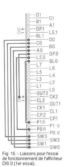
b) Perform the connections shown in Figure 15.
c) Set the four switches SW0, SW1, SW2 and SW3 to the 0 position.
d) Turn on the digilab.
On the DIS0 display, you must read the digit 0, as well as the decimal point on the right. If you do not get this result, check the connector group connections including soldering of the display brackets, if necessary, redo the soldering points.
Check that the + contact is at 5 volts.
If the decimal point does not light, check transistor T8.
Measure the voltage on its collector. You must find a voltage of the order of a tenth of a volt.
If you connect DP0 to ground, the collector voltage must exceed 3 volts.
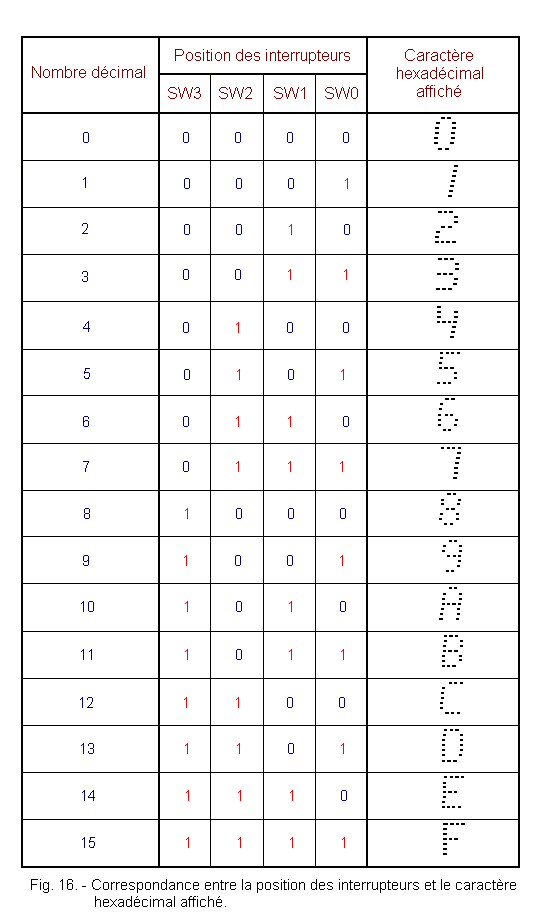
e) Put the four switches in the different positions shown in Figure 16.
In total, you have sixteen combinations to test.
For a given combination of the four switches, the corresponding hex character appears on the display.
Note that the Low Weight (LSB) bit is applied to the A input through the SW0 switch. The most significant bit (MSB) is applied to the D input.
Note also that the four switches SW0, SW1, SW2 and SW3 are respectively associated with the weight numbers 1, 2, 4 and 8.
This allows you to position the appropriate switches at position 1 to display the hexadecimal character you want.
For example, you set SW0 and SW3 to position 1. The displayed character is 9 (1 + 8 = 9).
If you set SW1, SW2 and SW3 to position 1, the displayed character is E (2 + 4 + 8 = 14).
Conversely, by reading any hex character on the display, simply "read" the position of the switches set to 1 to know the binary number associated with this hexadecimal character.
f) To check the operation of the LATCH circuit, press and hold the P0 button.
Change the switch combination and note that the display indication does not change.
g) By leaving the digilab on, eliminate the connection between DP0 and the + contact.The decimal point goes out.
h)Press P1. The erase control changes to H. The display goes off.
If you change the combination of the switches while keeping P1 pressed, you observe by releasing the P1 button that the display has taken into account the last combination of switches.
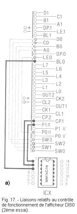
i) Eliminate the link between the contacts P1
and BL0 and make the new connections shown in Figure 17-a.
j) Insert the integrated circuit MM 74C08 (quadruple AND) into the ICX socket.
k) Put the four switches in any position.
The Figure 17-b shows the electrical circuit made.
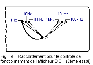
The clock signal at 1 Hz is applied to the erase input of the display through an AND logic gate.
The P1 button is used to validate the clock signal.
l) Press P1 and hold it as well. The hex character turns on and off once every second.
Now you will perform the same experiment by sending a clock signal at 100 Hz.
To do this, move the link between the COM 1 and 1 Hz contacts and put it between the COM 1 and 100 Hz contacts.
If you do not press P1, the hex character appears at full brightness.
If you press P1, the character always appears but its brightness decreases.
Indeed, now the character turns on and off 100 times per second, so this is not visible to the eye, but results in a decrease in brightness.
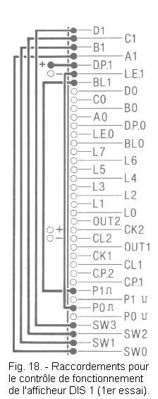
You will now check the operation of the display DIS 1. For this, you will resume the same tests from phase b) to phase l).
However, you will make new connections as shown in Figures 18 and 19, replacing Figures 15 and 17.
The contact of the right decimal point is indicated by the symbol DP1, the transistor used is T9 and the erase contact is identified by the initials BL1.
When the tests are complete, turn off the digilab.
To summarize, the displays mounted on the digilab are hexadecimal types and have a decoding circuit and a LATCH storage circuit.
These displays are therefore more sophisticated than some that require a decoder circuit outside.
During the next experiments, you will appreciate the ease of use of these displays.


 Description of TIL 311 displays
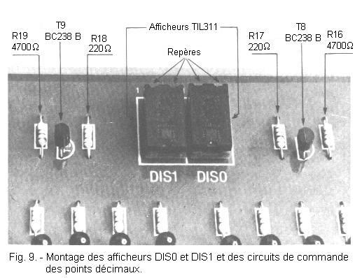


.gif)
.gif)
.jpg)
 Click here for the next lesson or in the summary provided for this purpose.
 Top of page
 Next Page