Approximations Successives 8 bits Analog / Digital Converter :
5. - FOURTH EXPERIENCE : EXAMINATION OF AN ANALOGUE / DIGITAL CONVERTER WITH SUCCESSIVE 8 BITS APPROXIMATIONS
It is an analog / digital converter built as an integrated circuit, it is the ADC 0804 circuit. On its input, we send an analog signal and we find the corresponding binary number on its output.
This circuit is made in CMOS technology and is quite complex. It can be used in a microprocessor system. The microprocessor indicates the beginning of an analog / digital conversion and the converter indicates the end of the conversion.
Before proceeding to its practical use, we will briefly see the operation of this A / D converter, whose block diagram is given in Figure 16.
At the beginning of the conversion, the control circuit generates a binary number corresponding to the value of the middle of the analog scale (1 000 0000 for an 8 bits converter).
A D / A circuit converts this number into an analog signal.
The comparator compares this signal with the input signal to be converted.
This comparator provides the control circuit with the result of the comparison.
At this time, the MSB is determined ; it is equal to 1 if the input signal is greater than the signal generated by the control circuit, it is 0 if it is not.
At this time, the control circuit generates a new binary number (0100 0000 or 1100 0000) which will make it possible to determine the value of the seventh bit (that located to the right of the MSB).
A new comparison phase takes place and the seventh bit is determined (0 or 1).
The process continues : the sixth bit is determined and so on until the LSB.
This method therefore makes it possible to approximate the theoretical binary number corresponding to the input analog voltage. In the present case, there are eight successive approximations. The resolution is 1 / 256 of the input voltage (with an 8 bits converter).
The binary number is read in the output register.
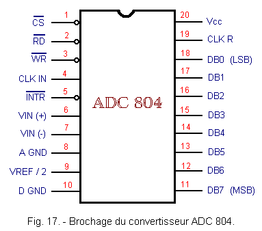
The converter has several control pins to manage its operation.
The beginning of conversion is carried out by applying a level L on the control terminal .
The terminal
makes it possible to validate the register of exit ; at the level H, the output is in the high impedance state ; at the level L, the contents of the output register is present on the output.
The output
signals the end of the conversion. For this, she goes to level L.
The entry
(Chip Select) allows you to select the converter. When it is at level L, the converter can operate.
The various steps (approximations) are carried out at the rate of a clock signal. An external clock signal applied to the CLK IN input can be used, or an assembly can be made with an external resistor and capacitor connected to a Schmitt trigger incorporated in the housing.
The analog signal is applied to the VIN (+) input. The other input VIN (-) can be either connected to the ground, be brought to a voltage allowing the setting of the converter at the beginning of scale, or be able to subtract a DC voltage from the input signal.
The pinout of the integrated circuit is given in Figure 17.
There are two pins for the ground : A GND and D GND.
A GND is the analog mass and D GND is the digital mass.
There are two different masses because the operation of the digital circuits can disturb that of the analog circuits, so it is preferred to have separate masses for each of these two parts of the integrated circuit.
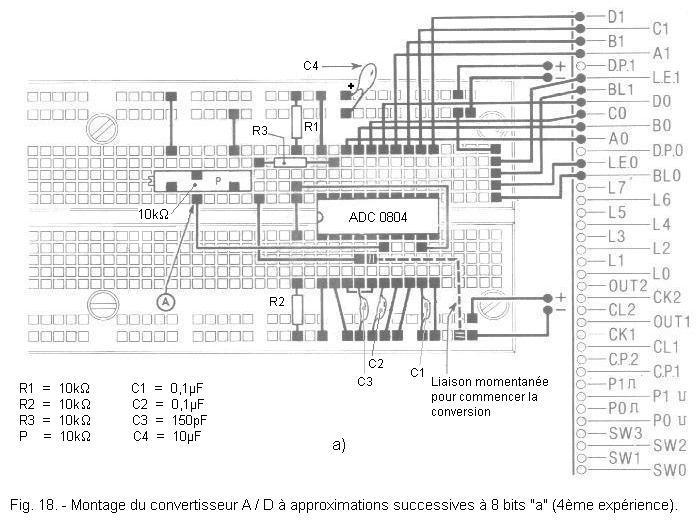
5. 1. - REALIZATION OF THE CIRCUIT
a) Remove from the matrix all the components and connections related to the previous experiment.
b) Insert on the matrix the integrated circuit ADC 0804, the potentiometric trimmer of 10 kΩ, three resistors of 10 kΩ, two capacitors of 0,1 µF, a capacitor of 150 pF and a tantalum electrolytic capacitor of 10 µF in the position indicated Figure 18-a.
c) Make the connections indicated in this same figure.
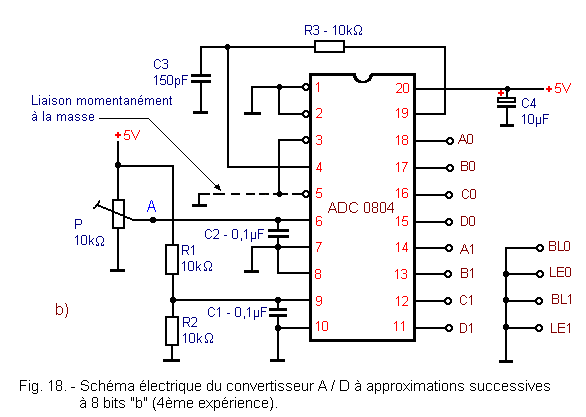
The electrical diagram of the realized circuit is given in Figure 18-b.
5. 2. - OPERATING TEST
a) Turn on the digilab.
b) Prepare the controller for continuous voltage measurements on the 10 volts gauge.
c) Put the positive tip in contact with point A corresponding to the potentiometer slider (Figure 18-a) and the negative touch point to ground.
d) Using the potentiometer slider P, move the voltmeter needle to 5 volts.
e) Connect for a moment to ground the pin 5 of the converter momentarily making the link indicated in dotted line in Figure 18-a. The converter is thus ready for operation.
f) Remove the link previously placed between pin 5 and ground.
The converter starts the conversion.
g) Both displays indicate a value close to FF. So, at the output of the converter, we have a binary number close to 1111 1111.
h) Operate the potentiometer slider P, so as to decrease the voltage at the input of the converter. For each new binary number, note the corresponding voltage.
This way, you can plot the transfer characteristic of the converter (or only part of it).
There are 256 combinations at the output of the converter, so the transfer feature is "a staircase of 256 steps".
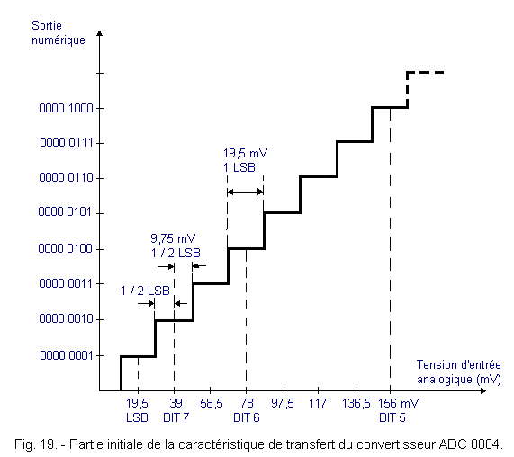
In Figure 19, the initial portion of this feature is shown.
You can note the voltages corresponding to the least significant bits (LSB, Bits 7, 6 and 5).
With the complete characteristic, it is possible to determine any binary number corresponding to a given voltage.
For example, for an input voltage of 156 mV, the output indicates the binary number 0000 1000 or 08 in hexadecimal. For 78 mV, the corresponding binary number is 0000 0100 or 0416.
The tables in Figures 20 and 21 allow you to easily convert the displayed value into the corresponding analog voltage.
Fig. 20. - Table
indicating the correspondence between the data display DIS0 and the value of the analog voltage. (Back to the lesson)
Indication of DIS0 display
Corresponding bit value
End of scale fraction
Input voltage (in volts)
End of scale = 5 volts
Vref / 2 = 2,5 volts
0
0000
0
0
1
0001
1 / 256
0,0195
2
0010
2 / 256
0,039
3
0011
3 / 256
0,0585
4
0100
4 / 256
0,078
5
0101
5 / 256
0,0975
6
0110
6 / 256
0,117
7
0111
7 / 256
0,1365
8
1000
8 / 256
0,156
9
1001
9 / 256
0,1755
A
1010
10 / 256
0,195
B
1011
11 / 256
0,2145
C
1100
12 / 256
0,234
D
1101
13 / 256
0,2535
E
1110
14 / 256
0,273
F
1111
15 / 256
0,2925
To do this, simply read the indications of the two displays and then look at the corresponding analog voltage in both tables.
Fig. 21. - Table
indicating the correspondence between the DIS1
display data and the value of the input analog voltage. (Back to the lesson)
Indication of DIS1 display
Corresponding bit value
End of scale fraction
Input voltage (in volts)
End of scale = 5 volts
Vref / 2 = 2,5 volts
0
0000
0
0
1
0001
1 / 16
0,3125
2
0010
2 / 16
0,625
3
0011
3 / 16
0,9375
4
0100
4 / 16
1,25
5
0101
5 / 16
1,5625
6
0110
6 / 16
1,875
7
0111
7 / 16
2,1875
8
1000
8 / 16
2,5
9
1001
9 / 16
2,8125
A
1010
10 / 16
3,125
B
1011
11 / 16
3,4375
C
1100
12 / 16
3,75
D
1101
13 / 16
4,0625
E
1110
14 / 16
4,375
F
1111
15 / 16
4,6875
It is sufficient to determine to sum the two voltages found in the tables.
For example, if the displays indicate C3 (C for DIS1 and 3 for DIS0), we can note in the first table that 3 corresponds to 0.0585 volt and in the second that C corresponds to 3.75 volts.
The input analog voltage is :
3,75 + 0,0585 = 3,8085 volts
Generally, you will not find the same value for the voltmeter indication and display indication.
First, the accuracy of the voltmeter intervenes.
Then there are two causes attributable to the converter.
The first may be an error of the reference voltage applied to the pin 9 of the integrated circuit (Figure 18-b).
In this case, the theoretical voltage should be 2.5 volts. For this purpose a resistance bridge consisting of R1 and R2 is used.
However, the supply voltage may be a little different from 5 volts and the two resistors R1 and R2 may have equally different values.
As a result, the reference voltage may be slightly different from 2.5 volts.
The second is the accuracy of the converter which is equal to ± 1 LSB in the present case.
We will define this notion.
Recall the "weight" of each bit.
BIT
WEIGHT (in Volt)
MSB
2,5
Bit 2
1,25
Bit 3
0,625
Bit 4
0,3125
Bit 5
0,156
Bit 6
0,078
Bit 7
0,039
LSB
0,0195
Looking at Figure 19, you notice that each numeric value corresponds to a plateau whose central value is expressed in volts.
Each bearing is 19.5 mV wide, which corresponds to the analog range of the LSB.
Thus, for each level, on either side of the central value, there is 1 / 2 LSB.
All analog voltage values between these two extremes (center value - 1 / 2 LSB and center value + 1 / 2 LSB) correspond to the same binary number.
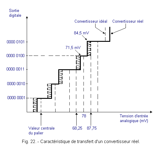
Figure 22 shows a real transfer characteristic.
Each bearing is no longer centered with respect to the central value on the one hand, and the width of the bearings is no longer constant on the other hand.
Thus, for a voltage corresponding to a shaded area, the binary value will be inaccurate. An example is shown in this figure.
Any voltage between 68.25 mV and 87.75 mV should be 0000 0100 in the ideal case. However, the bearing is reduced to the range of 71.5 mV to 84.5 mV in the real case. It follows that at a voltage between 68.25 mV and 71.5 mV will correspond to 0000 0011 and not to 0000 0100.
We will now define the accuracy of a converter.
It is expressed in fraction of LSB (example : precision of ± 1 / 4 LSB).
For an analog / digital converter, the precision, expressed in LSB fraction is the maximum difference existing between a vertical segment which connects two successive stages and the theoretical position of this vertical segment.
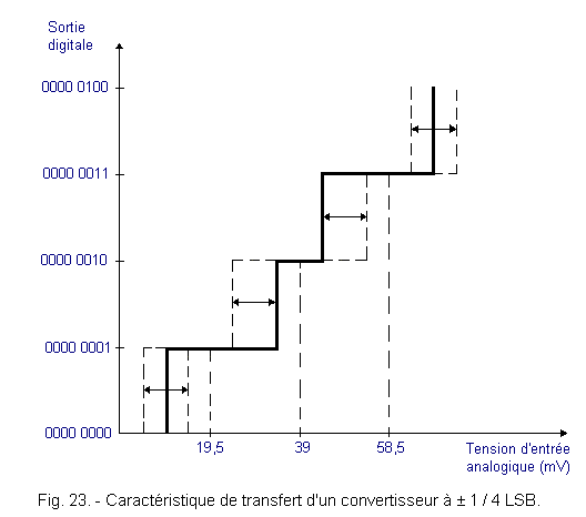
Consider the case of the converter having ± 1 / 4 LSB.
Looking at
the transfer characteristic of Figure 22, you observe that on either side of the 78 mV central value are theoretically two vertical segments at 68.25 mV and 87.25 mV respectively.
The accuracy ± 1 / 4 LSB corresponds to ± 1 / 4 x 19.5 mV, see ± 4.875 mV.
The first real segment should therefore not be more than 4,875 mV from the theoretical value of 68.25 mV.
It must be in an area between 68.25 - 4.875, or 63.375 mV and 68.25 ± 4.875, or 73.125 mV.
The calculation is similar for the second vertical segment.
Figure 23 shows the transfer characteristic of a ± 1 / 4 LSB converter.
The arrows indicate the areas where the vertical segments should be located.
The more accurate a converter is, the smaller the width of these areas.
If it were possible to design a converter with an accuracy of 0 LSB, the width of this zone would be zero and the transfer characteristic would be that of Figure 19 (ideal characteristic).
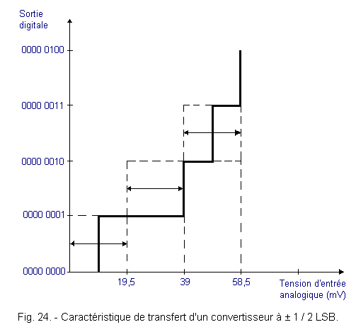
Figure 24 shows the characteristic of a ± 1 / 2 LSB converter.
The ADC 0804 converter has an accuracy of ± 1 LSB. The width of the area where a vertical front is located is 2 LSB or 39 mV.
There are more accurate converters, the type ADC 0801 is accurate to ± 1 / 4 LSB, the types ADC 0802 and ADC 0803 are accurate to ± 1 / 2 LSB.
You come to calculate the accuracy of the converter in your possession using the transfer characteristic. It suffices to calculate the maximum difference between the real vertical segments and the corresponding theoretical values.
In principle, calculate the gap for all vertical segments and take the largest one to determine accuracy.
i) After the experiment is complete, turn off the digilab.
We will summarize the main features of the circuit under consideration.
The analog voltage is applied to the input VIN (+), the other input VIN (-) is connected to ground.
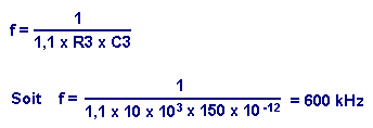
The two external components R3 and C3 define a clock frequency equal to :
Capacitors C1 and C2, connected to pins 9 and 6, serve to eliminate any parasites.
The reference voltage is obtained by means of a divider bridge consisting of R1 and R2.
The converter works repeatedly. As soon as one conversion is finished, another one begins again. For this, the output
(pin 5) is connected to the entry
(pin 3).
With a negative impulse on the entry ,
the conversion starts and the output
passes to the level L at the end of the conversion. However, this has the consequence of bringing the entry
to the level L and a new conversion starts again.
The conversion requires eight clock cycles plus a few additional cycles for the control circuit.
Experimented editing is impractical because the reading is done in hexadecimal code.
For the realization of a digital voltmeter, this type of converter is not suitable.
For this type of embodiment, the double-ramp conversion technique is generally adopted, which makes it possible to obtain a very high measuring accuracy. However, this technique is slower and is not suitable for converters to work at high frequencies.
In conclusion, we can say that each application requires a suitable converter. The one we looked at is very fast and it works in binary code, so it can easily be connected to a microprocessor.


 Footer
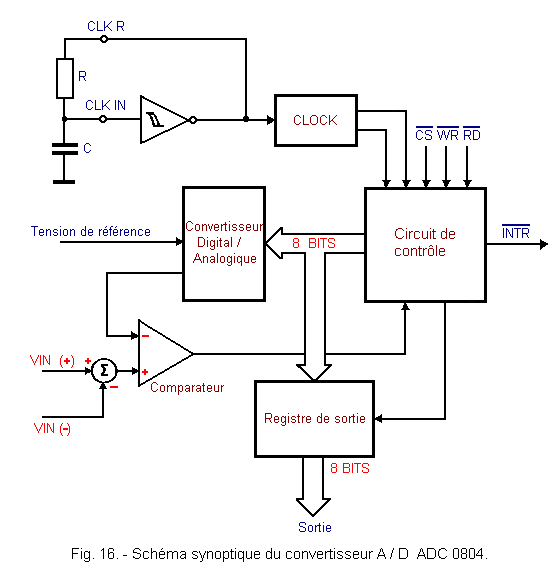
 Click here for the next lesson or in the summary provided for this purpose.
 Top of page
 Next Page